Double Duty: FPGA Architecture to Enable Concurrent LUT and Adder Chain Usage
By Junius Pun 1, Xilai Dai 2, Grace Zgheib 3, Mahesh A. Iyer 3, Andrew Boutros 4, Vaughn Betz 5, Mohamed S. Abdelfattah 2
1 Nanyang Technological University
2 Cornell University
3 Altera
4 University of Waterloo
5 University of Toronto
Abstract
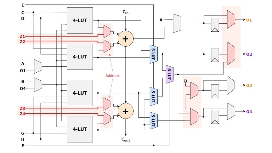
Flexibility and customization are key strengths of Field-Programmable Gate Arrays (FPGAs) when compared to other computing devices. For instance, FPGAs can efficiently implement arbitrary-precision arithmetic operations, and can perform aggressive synthesis optimizations to eliminate ineffectual operations. Motivated by sparsity and mixed-precision in deep neural networks (DNNs), we investigate how to optimize the current logic block architecture to increase its arithmetic density. We find that modern FPGA logic block architectures prevent the independent use of adder chains, and instead only allow adder chain inputs to be fed by look-up table (LUT) outputs. This only allows one of the two primitives -- either adders or LUTs -- to be used independently in one logic element and prevents their concurrent use, hampering area optimizations. In this work, we propose the Double Duty logic block architecture to enable the concurrent use of the adders and LUTs within a logic element. Without adding expensive logic cluster inputs, we use 4 of the existing inputs to bypass the LUTs and connect directly to the adder chain inputs. We accurately model our changes at both the circuit and CAD levels using open-source FPGA development tools. Our experimental evaluation on a Stratix-10-like architecture demonstrates area reductions of 21.6% on adder-intensive circuits from the Kratos benchmarks, and 9.3% and 8.2% on the more general Koios and VTR benchmarks respectively. These area improvements come without an impact to critical path delay, demonstrating that higher density is feasible on modern FPGA architectures by adding more flexibility in how the adder chain is used. Averaged across all circuits from our three evaluated benchmark set, our Double Duty FPGA architecture improves area-delay product by 9.7%.
To read the full article, click here
Related Semiconductor IP
- UMC 55nm ULP 3.3V Temperature Sensor
- High-Throughput Multi-Channel DMA Controller
- Configurable Multi-Channel DMA Controller
- Fixed-Channel Multi-Channel DMA Controller
- Verification IP for MIPI SoundWire
Related Articles
- LTE Single Carrier DFT: Faster Circuits with Reduced FPGA LUT/Register Usage
- Is FPGA power design ready for concurrent engineering?
- How to Reduce FPGA Logic Cell Usage by >x5 for Floating-Point FFTs
- How FPGA technology is evolving to meet new mid-range system requirements
Latest Articles
- Cryogenic Recharacterization of a Commercial 22 nm FD-SOI Foundry Standard-Cell Library
- A 105 MS/s 4.18 nJ/inference 0.765 mm² Mixed-Signal Streaming ML Engine for Wireless Baseband in 12LP+ FinFET
- Agentic AI for Heterogeneous System Design Across Chip, Scale-Up, and Scale-Out Domains
- Minimum RISC-V: Maximum FPGA Efficiency
- The Era of Vibe Tapeout: Dark Age or Golden Age for Analog Circuit Design?