Overview
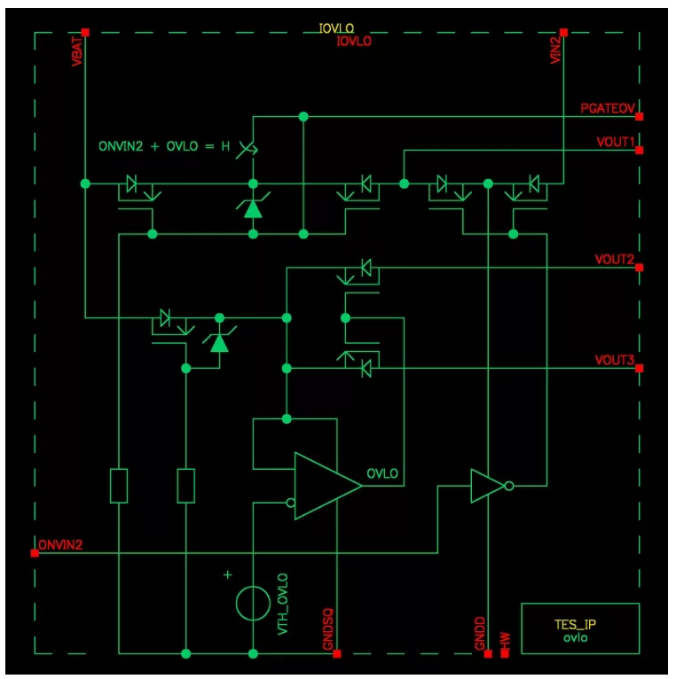
The TS_OVLO_3V3_X8 protects battery-operated circuits against damage when they are exposed to risks of their supply connector accidentally being wired to higher or wrong-polarity voltages, with extremes at ±30V. When battery-side input VBAT receives a voltage outside the range from 0V to typically +3.53V, the OVLO breaks the current paths to the three outputs VOUT1, VOUT2 and VOUT3.
When VBAT voltage is valid, the TS_OVLO_3V3_X8 draws as little current as 950nA maximum over the air temperature range from -40°C up to +85°C, which is ideal for battery longevity during shutdown periods. The on-state resistance to outputs VOUT2 and VOUT3 is 65Ω maximum for low battery voltage at +2.1V. The on-state resistance to output VOUT1 is 3Ω maximum and it can be further reduced by placing external PMOS switches in parallel, of which the gate is driven by control output PGATEOV.
The TS_OVLO_3V3_X8 contains a multiplexer that switches output VOUT1 over to system-side power input VIN2 when control input ONVIN2 is pulled up and provided that its voltage is regulated to 3.3V±0.1V. The corresponding on-state resistance is 1Ω maximum over the junction temperature range from -40°C up to +150°C.
The minimum continuous operation lifetime spans 100000 hours.
Technology: X-FAB XT018-0.18µm BCD-on-SOI CMOS
OPERATING CONDITIONS
| Parameters |
Values / Type |
| Temperature ranges |
Air, TA: -40ºC up to +85ºC
Junction, TJ: -40ºC up to +150ºC |
| Power input voltages with respect to ground GNDD and GNDSQ |
VBAT : -30V up to +30V
VIN2 : 3.2V up to 5.5V |
| ONVIN2 H-level voltage |
VIN2 |
SPECIFICATION
| Parameters |
Values |
| VTH_OVLO, Overvoltage-Lockout threshold |
+3.53V typ. (+3.56V max, +3.34V min) |
| RON_VBAT_VOUT1, VBAT to VOUT1 on-state resistance, ONVIN2 = L |
3Ω max at 2.1V |
| RON_VBAT_VOUT23, VBAT to VOUT2,3 on-state resistance |
65Ω max at 2.1V |
| RON_VIN2_VOUT1, VIN2 to VOUT1 on-state resistance, ONVIN2 = H |
1Ω max at 3.2V |
| ROFF_ VIN2_VOUT1, VIN2 to VOUT1 off-state resistance ONVIN2 = L |
50MΩ min |
| I_VBAT_30VREVERSE, reverse current through VBAT at -30V |
-50nA min, -1nA max |
| Current consumptions |
VBAT : 950nA max at +3.3V
VIN2 : 98µA max at 3.4V and ONVIN2 = H |
| Area |
0.455mm² |
Learn more about Power Management Unit IP core
TES Electronic Solutions GmbH announces the availability of TS_XOSC_32k_X8, a low-power 32.768 kHz Pierce crystal oscillator IP designed to provide a reliable low-frequency timing reference for battery-powered ASICs and system-on-chip (SoC) applications.
TES Electronic Solutions GmbH announces the availability of its DC-DC converter IP, TS_SWC_DCDC_3V6_X8, a 3.6 V boost‑buck converter that can be powered from a 2.5 V - 5.5 V supply voltage.
To meet the growing graphics demands, the industry is shifting toward scalable, shader programmable architectures. Unlike fixed-function graphics accelerators, shader programmable GPUs offer the flexibility required to target diverse market segments and at the same time ensure software portability and maintainability. Furthermore, adopting platform-independent stacks based on industry standards allows accelerating time-to market by developing applications on standard PC platforms before deployment to target hardware. TES Electronic Solutions in Germany addresses these challenges with the D/AVE NX GPU core. Engineered specifically for resource-constrained environments, it supports OpenGL ES 2.0 shader programmability with selected 3.x and vector graphics extensions.
TES Electronic Solutions GmbH offers TS_OVLO_3V3_X8 which is a compact Over-Voltage Lockout (OVLO) IP designed to protect battery-powered electronic systems against over-voltage and reverse-polarity faults of up to ±30 V.
A new DC-DC Split-Pi Boost-Buck Converter IP is released to offer designers a simple way to achieve high efficiency and precise regulation. TS_SPLITPI_3V3_X8 is a cascaded 3.3 V boost‑buck converter that can be powered from either a 10 V - 30 V supply or a low-voltage backup battery.
TES Electronic Solutions GmbH offers two new voltage buffer IPs with driving capabilities up to 6 mA, built on X-FAB’s XT018-0.18µm BCD-on-SOI process and operate across a junction temperature range of -40°C to 150°C with a supply voltage of 3.2V to 3.4V.