Vendor: NTLab Category: Single-Protocol PHY

1.2 Gbps LVDS transmitter/receiver

The interface to the core logic in receiver mode includes the signal pins (out_p and out_n) to receive data and the control pins …

TSMC 180nm BCDG2 Pre-Silicon View all specifications

Overview

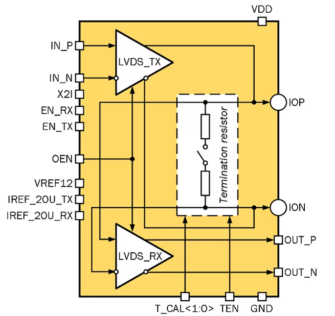
The interface to the core logic in receiver mode includes the signal pins (out_p and out_n) to receive data and the control pins (en_rx, ten, t_cal<1:0, oen) to configure the state of the receiver.
The interface to the core logic in transmitter mode includes the signal pins (in_p and in_n) to transmit data and the control pins (en_tx, x2i) to configure the state of the transmitter.
There are other two internal pins (vref12 and iref_20u_tx, iref_20u_rx) to get voltage reference and current references. IOP and ION are complementary pins to connect to the bonding pads. LVDS transceiver cell may be used for half-duplex data transmission. In this case, input oen controls the direction of the transmission (en_tx=1, en_rx=1). When oen = 1, block operates in the receiver mode –the transmitter output is in high impedance state. When oen = 0, block operates in the transmitter mode. In this case, the transmitter drives its output current into the differential LVDS line, with the polarity corresponding to the bit value being transmitted. This LVDS driver provides a double current mode (x2i=1) for system designs that employ double termination (near-end and far-end) of the differential signaling lines. Control pins (en_tx and en_rx) enable or disable transmitter and receiver. When en_tx=0, en_rx=1, block operates in the receiver mode –the transmitter output is in high impedance state and transmitter is disable. When en_tx=1, en_rx=0, block operates in the transmitter mode, receiver is disable. Block also comprises internal termination resistor with adjustable value. Input bits t_cal<1:0> are used for adjusting the termination resistance. The design target is to compensate 100 ohm resistance deviation from 20% to 10%. In order to use an external termination, the internal resistor may be switched off by setting low input ten.
The block is designed on TSMC 180 nm CMOS technology.
Key features

  • TSMC CMOS 180 nm
  • 3.3 V power supply
  • 1.2 Gbps (DDR MODE) switching rates (600 MHz)
  • Half-duplex or full-duplex operation mode
  • Conforms to TIA/EIA-644 LVDS standards without hysteresis
  • Temperature range: -60 °C to + 100 °C
  • Optimized for pad-limited layout design
  • Portable to other technologies (upon request)

Block Diagram

Applications

  • Point-to-point data receiver
  • Point-to-point data transmission
  • Multidrop buses
  • Clock distribution
  • Backplane data receiver
  • Backplane data transmission
  • Cable data receiver
  • Cable data transmission

What’s Included?

  • Schematic or NetList
  • Abstract model (.lef and .lib files)
  • Layout view (optional)
  • Behavioral model (Verilog)
  • Extracted view (optional)
  • GDSII
  • DRC, LVS, antenna report
  • Test bench with saved configurations (optional)
  • Documentation

Silicon Options

Foundry Node Process Maturity
TSMC 180nm BCDG2 Pre-Silicon

Specifications

Identity

Part Number
180TSMC_LVDS_09
Vendor
NTLab
Type
Silicon IP

Files

Note: some files may require an NDA depending on provider policy.

Provider

HQ: Lithuania

Learn more about Single-Protocol PHY IP core

UFS Goes Mainstream

UniversalFlash Storage (UFS) was created for mobile applications and computer systems requiring high performance and low power consumption. These systems typically use embedded Flash based on the JEDEC standard eMMC. UFS was defined by JEDEC as the evolutionary replacement for eMMC offering significantly higher memory bandwidth. The standard builds on existing standards such as the SCSI command set, the MIPI Alliance M-PHY and UniPro as well as eMMC form factors to simplify adoption and development.

Design IP Faster: Introducing the C~ High-Level Language

In this paper, we introduce a new high-level, dataflow programming language called C~ (“C flow”) that further increases productivity by raising the level of abstraction from behavioral descriptions, while overcoming the limitations of C for hardware design. We present the syntax and semantics of this language, and the framework that provides hardware and software code generation. This paper illustrates the benefits of using C~ for hardware design of a IEEE 802.3 MAC, synthesized for FPGA and for 90nm CMOS technology.

Universal Flash Storage: Mobilize Your Data

Universal Flash Storage (UFS) was created for mobile applications and computer systems requiring high performance and low power consumption. These systems typically use embedded Flash based on the JEDEC standard eMMC. UFS was defined by JEDEC as the evolutionary replacement for eMMC offering significantly higher memory bandwidth. The standard builds on existing standards such as the SCSI command set, the MIPI Alliance M-PHY and UniProSM as well as eMMC form factors to simplify adoption and development.

Can MIPI and MDDI Co-Exist?

Since MIPI and MDDI standards both target interfaces to cameras and displays on mobile devices, are two separate standards really needed?

Frequently asked questions about Single-Protocol PHY IP

What is 1.2 Gbps LVDS transmitter/receiver?

1.2 Gbps LVDS transmitter/receiver is a Single-Protocol PHY IP core from NTLab listed on Semi IP Hub. It is listed with support for tsmc Pre-Silicon.

How should engineers evaluate this Single-Protocol PHY?

Engineers should review the overview, key features, supported foundries and nodes, maturity, deliverables, and provider information before shortlisting this Single-Protocol PHY IP.

Can this semiconductor IP be compared with similar products?

Yes. Buyers can compare this product with similar semiconductor IP cores or IP families based on category, provider, process options, and structured technical specifications.

×
Semiconductor IP