Overview
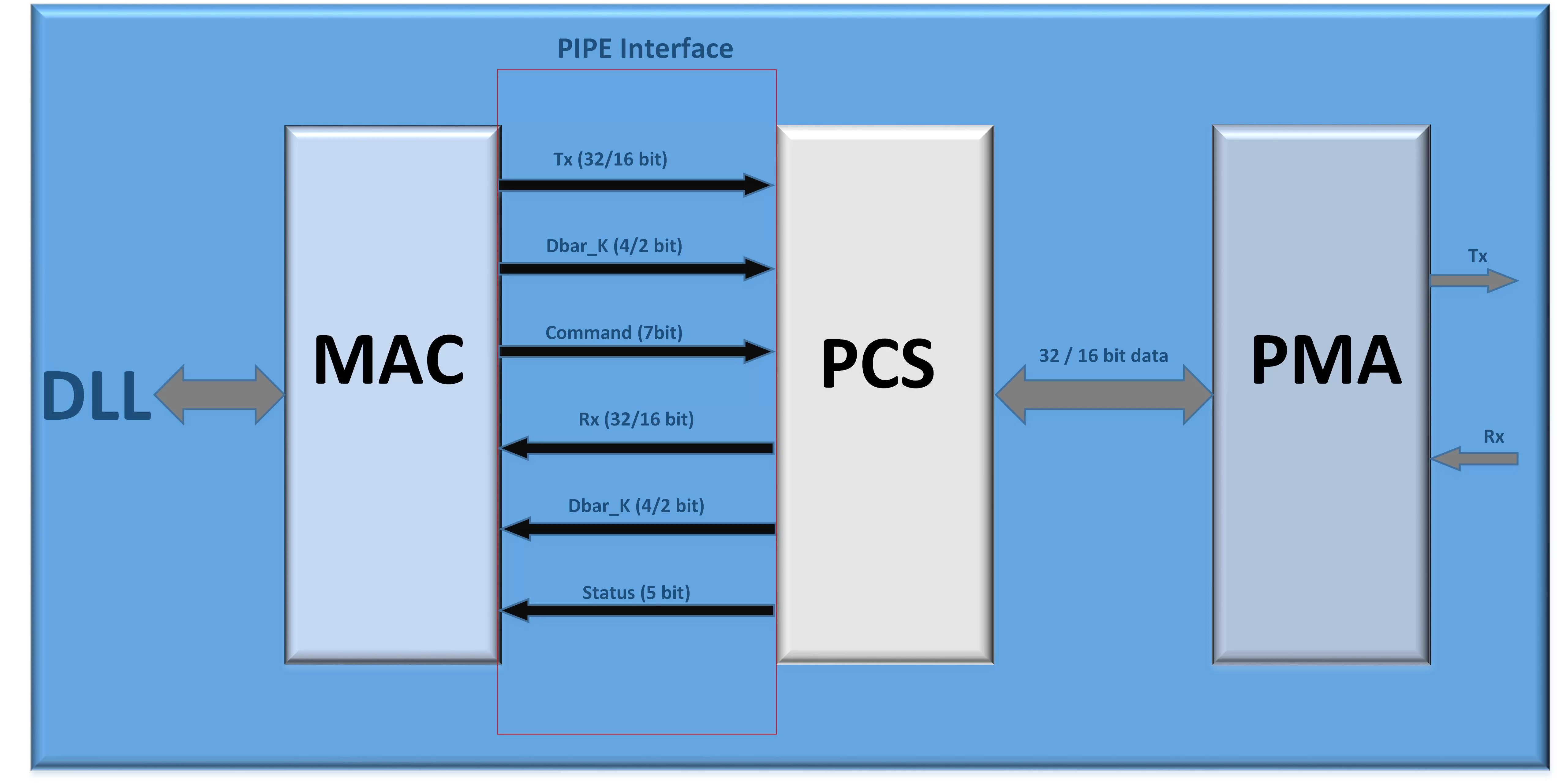
Atria Logic Pvt. Ltd. provides the complete design services for PCI Express. (2.5GT/s, 5GT/s) Our expertise covers the breadth of PCI-SIG's 3.0 specification of PCIe. We have a highly skilled team of experts who can deliver the services on PCIe physical layer including
- MAC
- PCS
- PIPE interface (8 bit, 16 bit and 32 bit interface)
- Scrambler
The PHY layer is essentially the PIPE (Physical Interface for PCIe Express). The designed PIPE interface follows the INTEL's PIPE spec. This Intel's spec is being used by other vendors like Xilinx, Altera and PLDA with slight modifications in LTSSM and power management states. However the basic Interface mentioned in Intel's spec is maintained by all vendors and so our design.
Architecture
The main goal of Physical Layer is to establish the physical connection or channel for proper communication of transactions coming from above layer (Transaction Layer and Data Link Layer).
The main functions of Tx side of PHY layer are listed below
- Link training through ordered sets TS1 & TS2
- Insertion of SKP ordered sets every 1538 symbols for elastic buffer overflow/underflow management.
- Sending Logical Idles in particular state of LTSSM and whenever there is no data available to send.
- Sending ElOS (Electrical Idle) as dictated by ASPM and Software Power management.
- Sending FTS(Fast Training Sequence) ordered sets whiling coming back to active state from Low power state.
- Generation of PIPE signals which includes
- Tx_data[32 or 16 bit]
- D/K [4 or 2bit]
- Tx_Elec_Idle
- Tx_Compliance
- Rate[1:0]
- Width [1:0]
- Pwr_dwn[2:0]
- Reset_PhY
- TxdetectRx
- Insertion of STP, SDP, END kontrol characters (Implemented in DLL)
All the Data packets except Kontrol characters and ordered sets will pass through scrambler.
Learn more about Single-Protocol PHY IP core
Numerous industries in broadcast, cable, videoconferencing and consumer electronics space are using H.264 as the video codec of choice for their products and services. The H.264/AVC video coding standard achieves a significant improvement in coding efficiency with increased computational complexity relative to former standards.
This article describes the use of a low-cost, low-density Zynq FPGA in creating a computational platform for implementing infotainment systems for passenger vehicles, such as cars, buses, trains, airplanes and ships. Other applications for this kind of platform include digital signage and information displays in private and public venues such as hotels, hospitals, gas pumps, or kiosks as well as digital picture frames for consumer markets.
With ever increasing need for very high operating frequency of graphics (GPU) or general purpose (CPU) processors, the limited memory bandwidth forms a bottleneck to extract maximum performance out of a system. To add to this, low power consumption, form factor of the memory devices also play significant roles in optimal and efficient solutions.
High Bandwidth Memory (HBM) is a high-performance 3D-stacked DRAM. It is a technology which stacks up DRAM chips (memory die) vertically on a high speed logic layer which are connected by vertical interconnect technology called TSV (through silicon via) which reduces the connectivity impedance and thereby total power consumption.