Agile Design for Hardware, Part II
David Patterson and Borivoje NikoliÄ, UC Berkeley
EETimes (7/30/2015 07:00 AM EDT)
In the second of a three-part series, two Berkeley professors suggest its time to apply Agile design techniques to hardware.
We asked readers of Part I to guess the cost of a prototype run of 28 nm chips, as Agile development relies on a sequence of interim prototypes versus the One Big Tapeout of the traditional Waterfall process. Here are the results:
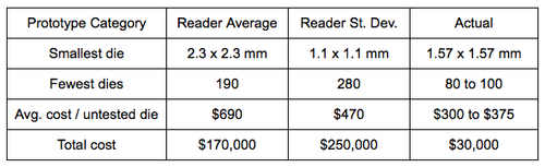
The surprisingly low manufacturing cost of prototype chips—one fifth the readers’ estimate—means Agile development is eminently affordable, even for academics. (See www.AgileSoC.com for more evidence.) It also calls into question the current high cost of designing SoCs using the Waterfall process. Having established Agile’s viability, based on our experience we propose four guidelines to lower development costs.
To read the full article, click here
Related Semiconductor IP
- Link Acceleration Unit
- 64-bit, RISC-V, ultra-high performance processors
- 64-bit, RISC-V, performance and data computation processors
- 32-bit, RISC-V, deeply embedded processors
- Verification IP for eUSB 2 v2 and USB 2.0
Related Articles
- Agile Design for Hardware, Part I
- How to design secure SoCs, Part II: Key Management
- QiMeng: Fully Automated Hardware and Software Design for Processor Chip
- LLMs for Secure Hardware Design and Related Problems: Opportunities and Challenges
Latest Articles
- Design and Development of a Neuromorphic Silicon Suite: PVT Sensing, Stochastic LIF Inference, On-Chip STDP Learning, and Crossbar Programming
- LLM4RTL: Tool-Assisted LLM for RTL Generation
- Towards Delta Aware Training: Efficient DNN Weight Storage for Resource-Constrained FPGAs
- CHERI-D: Secure and efficient inline object ID for CHERI temporal memory safety
- AIA: A 16nm Multicore SoC for Approximate Inference Acceleration Exploiting Non-normalized Knuth-Yao Sampling and Inter-Core Register Sharing