When Memory Shortages Change Architecture Decisions

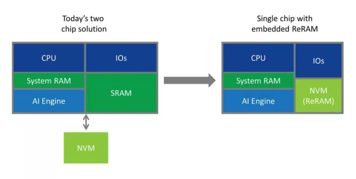
For decades, the choice between embedded and external Non-Volatile Memory (NVM) in semiconductor designs has been straightforward. External memory, such as EEPROM, NOR Flash, or NAND Flash, offered lower cost per bit and greater flexibility, making a two-die architecture the default choice across a wide range of applications.
That assumption is now being challenged.
A different kind of memory cycle
 The current memory market is not behaving like a typical pricing cycle. Driven by the rapid growth of AI infrastructure, memory vendors are prioritizing higher-margin segments such as HBM and data center DRAM. A growing share of global memory production (approaching 70%) is now being absorbed by data centers, tightening supply for other segments and creating a structurally constrained market for many traditional use cases.
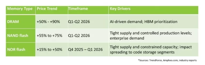
As a result, availability and pricing have become less predictable. Recent quarters have seen memory price increases of 50-90%, with further increases expected, while analysts project supply growth to remain below historical norms, extending shortages into 2027 and beyond.
Re-evaluating the two-chip model
For system designers, this introduces a new variable: supply risk. Memory is no longer just a line item in the bill of materials. It is a potential point of failure in the supply chain. In this environment, companies are revisiting a fundamental question: Does this system need external memory at all, or can it rely on embedded memory instead?
The traditional rationale for external memory (lower cost) doesn’t always hold when factoring in price volatility, lead time and allocation risk, additional packaging and board space, power consumption and latency, and other factors. Importantly, pricing pressure is not limited to high-density memory; it is increasingly affecting the low- and mid-density NOR devices commonly used for code storage, where redesign options can be more constrained due to tight coupling with boot architecture, execute-in-place (XiP) operation, and secure firmware storage. This can make it non-trivial to remove without architectural changes. When these issues are considered at the system level, the economy begins to shift.
In practice, many teams are already responding by minimizing external memory footprint, separating boot and bulk storage, and evaluating embedded alternatives earlier in the design cycle.
Where the shift is happening
The conditions are now aligned in a way that makes embedded NVM materially more attractive in specific segments, particularly where BOM (bill of materials) cost, supply risk, and power/latency matter, and where embedded NVM already has latent advantages.
This shift is obvious in microcontrollers (MCUs) and control SoCs. Designers of new systems are increasingly looking to eliminate external EEPROM or NOR, integrating non-volatile memory directly on chip to simplify design, reduce power and latency, and reduce cost and dependency on external components.
We are also seeing the shift in analog and power devices on BCD platforms. Designers of applications such as Power Management ICs (PMICs) are increasingly looking to integrate intelligence into their designs, effectively creating smart battery management systems and intelligent PMICs for wireless charging, motor control, and other high-voltage applications. Such designs require an integrated microcontroller with embedded NVM to store the code.
Automotive and industrial applications are also feeling the pinch. As these systems move to more advanced nodes, on-chip NVM becomes increasingly necessary to support higher speed and endurance requirements (often 100K cycles or more). External memory can become a bottleneck in this context, both in performance and in meeting endurance and security requirements. At the same time, long lifetimes and strict qualification requirements make additional components undesirable. Removing external memory can reduce failure points and simplify system validation, reinforcing the preference for single-die solutions. Supply chain instability and rising costs further reinforce this trend.
In edge AI and smart sensors, we are also seeing a shift. As more intelligence moves to the edge, the ability to store firmware or model weights on chips becomes increasingly valuable. External memory adds latency, power, and additional points of security risk. Embedded memory enables lower latency, lower power, and more compact system designs. And while this is less about shortages and more about architecture, pricing pressure accelerates the shift.
It is important to be precise about the scope of this shift. External memory will remain essential for high-density storage. And applications requiring large memory arrays or flexible configurations will continue to rely on discrete devices for some time. What is changing is the boundary. As system-level costs and risks are reassessed, the range of applications where embedded memory is the better choice is expanding.
Explore Embedded Memory IP:
The role of embedded ReRAM
As designers re-evaluate system architectures, embedded NVM is gaining attention not only as a cost-effective alternative, but as an enabler of simpler and more resilient designs. Among emerging technologies, ReRAM (RRAM) is particularly well aligned with these requirements. Because it can be integrated in the back-end-of-line (BEOL) using standard materials and equipment, it avoids many of the cost and complexity challenges associated with traditional embedded flash or other emerging memories. This enables:
- Minimal additional masks and process steps
- Compatibility with a wide range of CMOS nodes, including analog and BCD platforms
- Lower operating power and voltage
- Fast write performance and byte-level access without erase cycles
- Scaling below 28nm
These characteristics make it possible to embed NVM in applications where it was previously impractical, expanding the range of designs that can move to a single-chip architecture. This includes applications that have traditionally relied on external NOR for boot and code storage, where integration was previously impractical. As more designs migrate to advanced nodes, traditional embedded flash becomes increasingly difficult to integrate, as it does not scale effectively as an embedded technology below 28nm. This makes alternatives such as ReRAM a more practical option. Importantly, embedded ReRAM is no longer a research concept. It is now available as silicon-proven IP across multiple foundry processes, enabling designers to adopt it within standard development flows.
A structural change, not a temporary reaction
Memory shortages do more than increase prices; they influence architecture decisions. The upfront cost of redesign means transitions typically occur in new product generations, but once a system transitions from a two-chip to a single-chip solution, it rarely reverts. The benefits in integration, power, and reliability are persistent.
New capacity takes years to come online, extending the impact of today’s constraints. This means the current environment is likely to drive long-term changes in design approaches, not just short-term adjustments.
We are still in the early stages of this shift. Most of the impact will appear in future product generations, given the typical design cycle of semiconductor devices. However, the direction is clear. Designers are moving beyond a simple cost-per-bit comparison and taking a broader view of system efficiency and resilience. In that context, embedded non-volatile memory, and ReRAM in particular, is becoming a more compelling option across a growing set of applications.
Related Semiconductor IP
- ReRAM NVM in DB HiTek 130nm BCD
- ReRAM NVM in SkyWater 130nm
- ReRAM as FTP/OTP Memory
- ReRAM Secure Keys
Related Blogs
- Instant FPGA Fashion Change, Except When It Isn't
- Key Advantages of Synopsys Memory VIP Architecture
- When Considering Processor PPA, Don't Forget the Instruction Memory
- The Importance of Memory Architecture for AI SoCs
Latest Blogs
- M31 High-Speed and Long-Channel MIPI C/D-PHY Solution on TSMC N3P/N3C
- Understanding security certification and how analog IP can help
- Embedded Security explained: Secure boot for embedded systems
- World's First Standards-Compliant 112G PHY IP for Linear Optics: A Turning Point for AI Interconnects
- One Key for Every Door: How Aliro Extends the UWB Digital Key Beyond the Car