AI in Design Verification: From Experimentation to Measurable Capability

AI in design verification no longer asks if AI helps tasks, but does it measurably improve real verification flows?
AI in design verification, or “AI in DV”, has moved from speculative discussion into practical engineering trials. Verification teams are already examining AI-assisted approaches for regression triage, debug support, coverage analysis, failure clustering, log summarization, and knowledge retrieval.
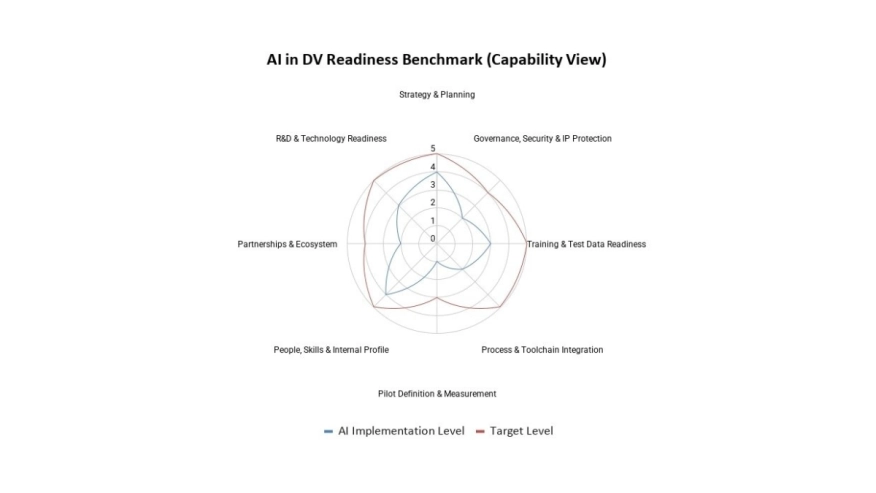 That shift is useful, but it also changes the question. The industry is no longer only asking whether AI can help with isolated tasks. In many bounded cases, it can. The more important question is whether “AI in DV” improves measurable verification capability inside real project flows.
This distinction matters because verification is not simply a productivity activity. It is a confidence-building discipline. The objective is not to produce more artefacts, tests, or reports. The objective is to reduce functional risk, close meaningful coverage gaps, preserve traceability, and support defensible signoff decisions. Industry studies continue to frame functional verification as a critical challenge as semiconductor design complexity grows [1]. That makes AI attractive, but it also means adoption must be judged by engineering outcomes rather than novelty.
To read the full article, click here
Related Semiconductor IP
- NPU IP
- JPEG XL Encoder
- I2C Master/Slave Controller Core
- NVMe Validation Test Suite
- Hybrid Memory Cube Verification IP
Related Blogs
- Reimagining Chip Design - From Spec to Signoff with Cadence AI Super Agents
- Verification Sanity in Chiplets & Edge AI: Avoid the “Second Design” Trap
- AI in Design Verification: Where It Works and Where It Doesn’t
- From DIY To Advanced NoC Solutions: The Future Of MCU Design
Latest Blogs
- Tape-Out Readiness Checklist: Engineering Decisions That Prevent Costly Respins
- How Cadence DSPs Put In-Cabin AI Audio On-Chip in SemiDrive's X10
- The Fastest Path to Scalable Photonic Systems: Using Proven IP for both PIC and EIC designs
- Building Trusted AI Agents from the Silicon Root of Trust
- Heterogeneous Computing in Space