AI can design the chip, manufacturing it is harder
October 30, 2026

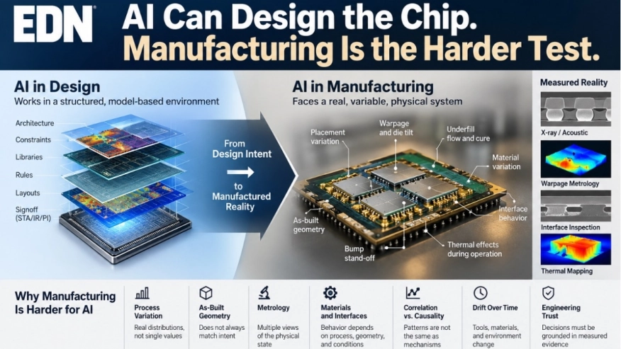 AI is getting better at navigating semiconductor design. It can search design spaces, optimize constraints, generate layouts, explore trade-offs, and increasingly interact with established EDA flows. But there is a major difference between designing a chip and manufacturing one.
Design lives primarily in a structured environment of models, rules, constraints, libraries, and solver outputs. Manufacturing does not; it creates a physical system. That physical system can vary from the intended design because of process conditions, materials, equipment behavior, geometry, assembly sequence, temperature, loading, and time.
To read the full article, click here
Related Semiconductor IP
- 100-10Gbps Ethernet MAC Controller
- SD Card Controller
- AXI4 Memory Controller IP Core
- AXI-Lite I2C Controller Core
- LVDS Transceiver IP core
Related Blogs
- What the steam engine can teach us about modern chip design
- The Missing Layer in AI Systems Design is Predictable, Scalable Data Movement
- Generative AI is changing the world - but can it continue to succeed with our current data infrastructure?
- Can AI-Driven Chip Design Meet the Challenges of Tomorrow?