Vendor: T2M GmbH Category: Multi-Protocol PHY

USB 3.0/ PCIe 2.0 Combo PHY IP, Silicon Proven in TSMC 28HPC+

The Combo PHY is a USB 3.0 and PCIe 2.0 PHY IP solution designed for a mobile and data consumer applications in TSMC 28nm process.

TSMC 28nm HPC+ In Production View all specifications

Overview

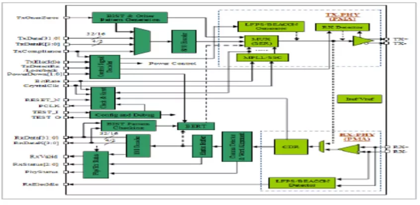
The Combo PHY is a complete USB 3.0 and PCIe 2.0 PHY IP solution designed for a mobile and data consumer applications in TSMC 28nm process. It supports both USB3.0 (1 or 2 ports) and PCIe 2.0 (1 lane). It consists of Physical Coding Sublayer and Physical Media Attachment and includes all circuitry for interface operation with 8/10 encoding/decoding, driver, input buffers, PLL and impedance matching circuitry. The PHY provides standard PIPE interface with the Media Access Layer for exchanging information. Lower power consumption is achieved due to support of additional PLL control, reference clock control, and embedded power gating control. Also, since aforementioned low power mode setting is configurable, the PHY is widely applicable for various scenarios under different consideration of power consumption.

Key features

  • Standard PHY interface (PIPE) enables multiple IP sources for PCIe/USB3 MAC layer
  • Supports 2.5GT/s and 5.0GT/s serial data transmission rate
  • Supports 16-bit or 32-bit parallel interface
  • Data and clock recovery from serial stream
  • 8b/10b encoder/decoder and error indication
  • Support direct disparity control for use in transmitting compliance pattern in Pole mode
  • Support power change and rate change at a same PCLK edge in PCIe mode
  • Tunable Receiver detection to detect worse case cables
  • Beacon transmission and reception in Pole mode
  • Low Frequency Periodic Signaling (LFPS) transmission and reception in USB 3.0 mode
  • Support SSCG function to reduce EMI effects with tunable down spread amplitude
  • Selectable TX margining, Tx de-emphasis and signal swing values
  • Internal Loopback Test Capable
  • Allowable analog circuit parameter adjustment and internal test control
  • Compliant with USB3/PCIe base specification
  • Silicon Proven in TSMC 28HPC+.

Block Diagram

What’s Included?

  • GDSII & layer map
  • Place-Route views (.LEF)
  • Liberty library (.lib)
  • Verilog behavior model
  • Netlist & SDF timing
  • Layout guidelines, application notes
  • LVS/DRC verification reports

Silicon Options

Foundry Node Process Maturity
TSMC 28nm HPC+ In Production

Specifications

Identity

Part Number
USB 3.0/ PCIe 2.0 Combo PHY IP in 28HPC+
Vendor
T2M GmbH
Type
Silicon IP

Files

Note: some files may require an NDA depending on provider policy.

Provider

T2M GmbH
T2M GmbH is the leading Global Technology Company supplying state of the art complex semiconductor connectivity IPs and KGDs, enabling the creation of complex connected devices for Mobile, IoT and Wearable markets. T2M's unique SoC White Box IPs are the design database of mass production RF connectivity chips supporting standards including Wifi, BT, BLE, Zigbee, NFC, LTE, GSM, GNS. They are available in source code as well as KGD for SIP / modules. With offices in USA, Europe, China, Taiwan, South Korea, Japan, Singapore and India, T2M’s highly experienced team provides local support, accelerating product development and Time 2 Market.

Learn more about Multi-Protocol PHY IP core

How a 16Gbps Multi-link, Multi-protocol SerDes PHY Can Transform Datacenter Connectivity

Increasingly, more of the focus on mobile has centered around cloud datacenters and the networking to get the data back and forth between these datacenters and the mobile device. Functions like voice recognition and mapping depend on the ability to split the functionality between the smartphone, for local processing like encryption and compression, and the back end, where a large number of servers can do the heavier lifting before returning the results.

One PHY, Zero Tradeoffs: Multi-Protocol PHY for Edge AI Interface Consolidation

The Cadence 10G multi-protocol PHY was architected to address this exact challenge. Designed to scale across multiple process nodes, it consolidates PCI Express (PCIe), USB, DisplayPort, Ethernet, and other interfaces into a single, compact, silicon-efficient block. What sets it apart is simultaneous multi-protocol support, which enables multiple data paths without duplicating hardware, requiring extra board connectors, or paying the area and power penalty of separate IP blocks.

Frequently asked questions about Multi-Protocol PHY IP cores

What is USB 3.0/ PCIe 2.0 Combo PHY IP, Silicon Proven in TSMC 28HPC+?

USB 3.0/ PCIe 2.0 Combo PHY IP, Silicon Proven in TSMC 28HPC+ is a Multi-Protocol PHY IP core from T2M GmbH listed on Semi IP Hub. It is listed with support for tsmc In Production.

How should engineers evaluate this Multi-Protocol PHY?

Engineers should review the overview, key features, supported foundries and nodes, maturity, deliverables, and provider information before shortlisting this Multi-Protocol PHY IP.

Can this semiconductor IP be compared with similar products?

Yes. Buyers can compare this product with similar semiconductor IP cores or IP families based on category, provider, process options, and structured technical specifications.

×
Semiconductor IP