Vendor: Cadence Design Systems, Inc. Category: LPDDR

LPDDR PHY and Controller

LPDDR6, LPDDR5X, LPDDR5, LPDDR4X, LPDDR4, LPDDR3 PHY and Controller

Overview

A Family of High-Speed On-Chip Memory Interface IP

The Cadence PHY and Controller for LPDDR6/5X/5/4X/4/3 is a family of high-speed on-chip memory interface IP that satisfy high-performance requirements with products that are optimized for each application's needs.

The latest LPDDR6/5X PHY and Controller IP support the newest JEDEC Low-Power Double Data Rate DRAM (LPDDR6) standard with data rates of up to 14.4Gbps, up to 50% faster than the previous generation. The LPDDR6/5X IP product line is a new high-speed architecture that is based on Cadence’s industry-leading LPDDR5X 10.7Gbps and GDDR6 22Gbps products. The architecture targets high-performance and artificial intelligence (AI) applications. The high-performance design features dynamic feedback equalization (DFE), feed forward equalization (FFE), and continuous time linear equalization (CTLE), as well as per-bit read and write delay adjustment. Cadence’s proprietary ultra-low jitter clock trees and DLLs, proven in the GDDR6 22Gbps product line, contribute to better system timing margins, lower cost package and PCB designs, and overall system reliability. Multiple low-power modes and configurations are supported and target industry-leading exit latencies, multiple frequency set points (FSP), and dynamic frequency scaling (DFS) in hardware.

The LPDDR6/5X IP products are designed to integrate easily into AI and data center applications. The PHY IP can be delivered as either firm or hard macros, supporting multiple floorplan and bump map options. The PHY top-level logic uses low clock frequencies to enable easier, faster, and more reliable timing closure.

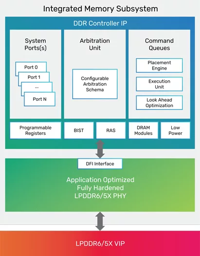
The LPDDR Controller delivers a wide array of capabilities to address emerging LPDDR DRAM subsystem RAS, ECC, parity, and data-scrubbing functions. The application-optimized LPDDR6 PHY and Controller can achieve industry-leading data rates, with low-power features that include multiple low-power states for longer battery life and greener operation.

Key features

PHY

  • Application-optimized configurations for fast time to delivery and lower risk
  • Low-power VDD idle, VDD light sleep, and power-efficient clocking in low-speed modes
  • I/O pads with impedance calibration logic and data-retention capability
  • Fine-grain custom delay cell for delay tuning
  • Internal and external datapath loop-back modes
  • RX and TX equalization for heavily loaded systems
  • Programmable per-bit (PVT compensated) deskew on read and write datapaths
  • Multiple floor plans

Controller

  • Memory controller interface complies with DFI standard
  • Application-optimized configurations for fast time to delivery and lower risk
  • Supports advanced RAS features including error scrubbing, parity, etc.
  • Compliant to LPDDR6/5X/4X/4/3 protocol memories
  • Priority per command on Arm®AMBA® 4 AXI, AMBA 3 AXI
  • Single and multi-port host interface options
  • QoS features allow command prioritization on Arm AMBA 4 AXI and CHI interfaces

Block Diagram

Benefits

  • High Performance: For AI/ML and targeted data center applications
  • Low Power and Area: Industry-leading PPA based on advanced architecture and implementation
  • Reliable: Maximum system margin with advanced clocking and I/O architectures

Specifications

Identity

Part Number
LPDDR PHY and Controller
Vendor
Cadence Design Systems, Inc.
Type
Silicon IP
Controller / PHY
Controller

Files

Note: some files may require an NDA depending on provider policy.

Provider

Learn more about LPDDR IP core

DDR5 MRDIMM Gen2: The Missing Link in Scaling AI Infrastructure

Cadence leads the market with its DDR5 MRDIMM 12.8 Gbps Gen2, TSMC N3P IP system solution, establishing a new benchmark for industry-leading PPA. Key industry leaders have already adopted this solution, which is now also available in the TSMC N2P and N5/N4P process nodes.

AI Semiconductor Design at 3nm and 2nm: Silicon-Proven IP

In this second blog of our ongoing series, we examine how Cadence, in close partnership with TSMC, helps teams accelerate AI silicon design at advanced process nodes. For customers, this translates into reduced design risk, faster convergence to tapeout‑quality results, and greater confidence at the leading edge of AI and HPC design.

DFI 6.0 Key Highlights of the Latest DFI Specification

DFI 6.0.1 (also referred to as DFI 6.0 in the rest of the blog) is the latest standard of the DFI specification. It removes support for earlier DDR/LPDDR generations, adds support for LPDDR6 and HBM4, adds/modifies low-power features, reorganizes WCK and memory-error handling, removes the disconnect protocol, and adds support for 1:3 and 1:6 DFI ratios.

SOCAMM: Modernizing Data Center Memory with LPDDR6/5X

Small Outline Compression-Attached Memory Module (SOCAMM) has made its way into the data center as an alternative to external CPU memory, due to its high performance, low power, memory capacity, and scalability.

Frequently asked questions about LPDDR Interface IP

What is LPDDR PHY and Controller?

LPDDR PHY and Controller is a LPDDR IP core from Cadence Design Systems, Inc. listed on Semi IP Hub.

How should engineers evaluate this LPDDR?

Engineers should review the overview, key features, supported foundries and nodes, maturity, deliverables, and provider information before shortlisting this LPDDR IP.

Can this semiconductor IP be compared with similar products?

Yes. Buyers can compare this product with similar semiconductor IP cores or IP families based on category, provider, process options, and structured technical specifications.

×
Semiconductor IP