Overview
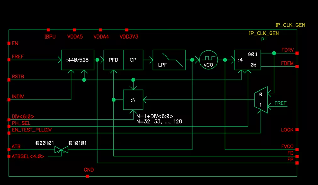
This integer-N PLL synthesizes 3.3V-square-wave FVCO frequencies within the HF range from 2.424MHz up to 9.697MHz, by steps of 18.9393kHz, and provides one fourth of fVCO on two other outputs, FDEM and FDRV, which feature quadrature phase difference or no phase shift depending on the control bit PH_SEL.
The PLL-locked state within ±0.08% of fVCO is signaled by a logic high level on the LOCK output.
The PLL operates with three supply voltages, VDDA5 (5V typical), VDDA4 (4V typical from the additional IP TS_VR_4V00_X8) for the analog and test-bus (ATB) circuits and VDD3V3 (3.3V typical from the additional IP TS_VR_3V30_X8) for the digital circuits.
The PLL is meant for on-chip internal operation. Its inputs or outputs that need access to bond pads will require the insertion of ESD-protected buffers. The ATB path complies with 2kV electrostatic discharges.
The minimum continuous operation lifetime spans 100000 hours.
Operating conditions
| Parameters |
Values |
| Junction temperature range |
20ºC to +80ºC |
| Supply voltages |
VDDA5: 4.9V to 5.1V
VDDA4: 3.9V to 4.1V (supplied by the additional IP Reg_4V)
VDD3V3: 3.2V to 3.4V (supplied by the additional IP Reg_3V3) |
| Reference sourced current intensity |
I(IBPU): 19.5µA to 20.5µA (supplied by the additional IP Bias) |
| FREF-input reference frequency |
8.333MHz or 10.000MHz |
Specification
| Parameters |
Values |
| FVCO-output frequency range |
2.424MHz to 9.697MHz |
| FVCO frequency step size |
18.9393kHz |
| FDRV-/FDEM-output frequency range |
606.06kHz to 2.424MHz |
| FVCO period jitter @2.424MHz |
271psRMS max |
| PLL lock time upon power on |
4.95ms max |
| LOCK response time to PLL-locked state |
150ms max |
| Operating power consumption Enable EN high, active-low reset RSTB high |
870µW max |
| Powerdown-mode current consumption Enable EN low |
187nA max |
| Area |
0.16mm² |
Learn more about PLL IP core
TES Electronic Solutions GmbH announces the availability of TS_XOSC_32k_X8, a low-power 32.768 kHz Pierce crystal oscillator IP designed to provide a reliable low-frequency timing reference for battery-powered ASICs and system-on-chip (SoC) applications.
TES Electronic Solutions GmbH announces the availability of its DC-DC converter IP, TS_SWC_DCDC_3V6_X8, a 3.6 V boost‑buck converter that can be powered from a 2.5 V - 5.5 V supply voltage.
To meet the growing graphics demands, the industry is shifting toward scalable, shader programmable architectures. Unlike fixed-function graphics accelerators, shader programmable GPUs offer the flexibility required to target diverse market segments and at the same time ensure software portability and maintainability. Furthermore, adopting platform-independent stacks based on industry standards allows accelerating time-to market by developing applications on standard PC platforms before deployment to target hardware. TES Electronic Solutions in Germany addresses these challenges with the D/AVE NX GPU core. Engineered specifically for resource-constrained environments, it supports OpenGL ES 2.0 shader programmability with selected 3.x and vector graphics extensions.
TES Electronic Solutions GmbH offers TS_OVLO_3V3_X8 which is a compact Over-Voltage Lockout (OVLO) IP designed to protect battery-powered electronic systems against over-voltage and reverse-polarity faults of up to ±30 V.
A new DC-DC Split-Pi Boost-Buck Converter IP is released to offer designers a simple way to achieve high efficiency and precise regulation. TS_SPLITPI_3V3_X8 is a cascaded 3.3 V boost‑buck converter that can be powered from either a 10 V - 30 V supply or a low-voltage backup battery.
TES Electronic Solutions GmbH offers two new voltage buffer IPs with driving capabilities up to 6 mA, built on X-FAB’s XT018-0.18µm BCD-on-SOI process and operate across a junction temperature range of -40°C to 150°C with a supply voltage of 3.2V to 3.4V.