Vendor: Cadence Design Systems, Inc. Category: USB

eUSB2V2 Controller

Proven solution featuring host and peripheral

Overview

Proven solution featuring host and peripheral

eUSB2V2 scales up to 4.8Gbps of data rate with the flexibility to configure asymmetrical or symmetrical links to build an efficient system, depending on the intended application. In asymmetrical link mode, one direction can achieve speeds of up to 4.8Gbps, while the reverse can operate at a lower rate of 480Mbps. This flexibility allows for simpler designs, optimized power consumption, and reduced EMI noise. Symmetrical links can be configured to run at speeds between 960Mbps and 4.8Gbps.

Key features

  • Meet low voltage requirement (1.0V – 1.2V)
  • Up to 4.8Gbps scalable data rate
  • Leverages existing USBSSP2 IP
  • Burst transactions improvement for Isochronous Endpoints
  • New MaxPacketSize for Bulk Endpoint (1024 bytes)
  • Support for Legacy Protocol (HS Native Mode) operation
  • Design flexibility with both asymmetrical and symmetrical links
  • Configurable number of eUSB2V2 Ports
  • No change in existing USB2/USB3 Port

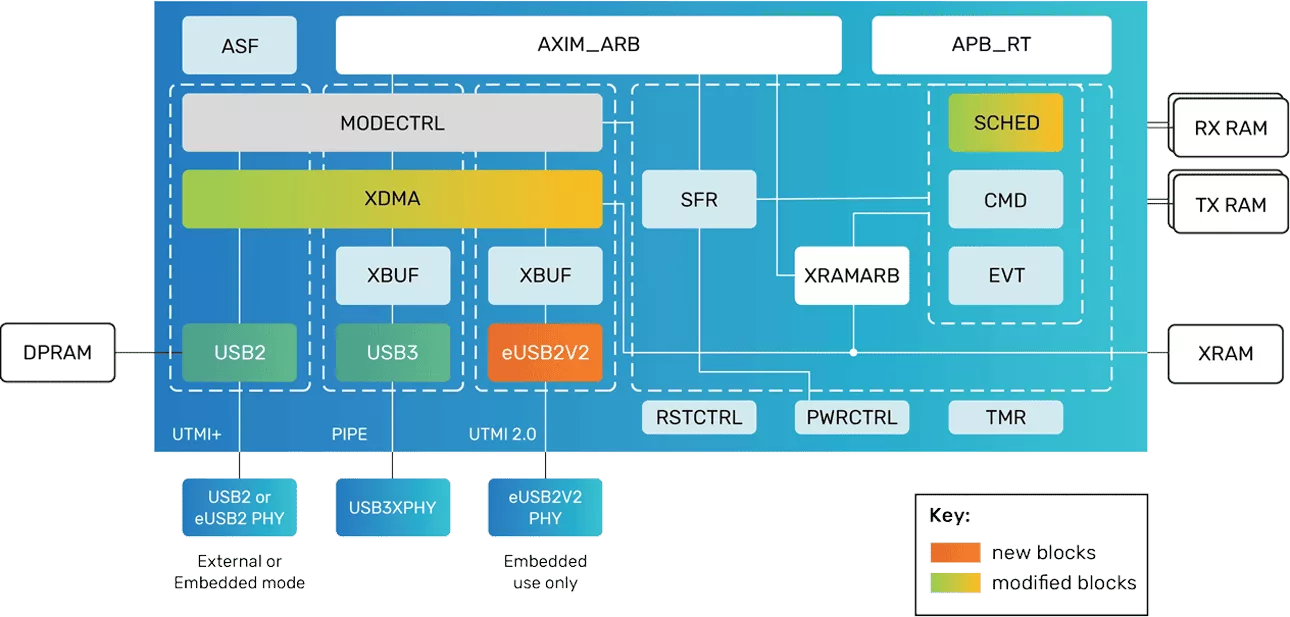
Block Diagram

Benefits

  • Complete IP Solution: PHY + Controller + Driver + VIP facilitates rapid SoC development
  • Scale up to 4.8Gbps of Data Rate: Support both symmetrical and asymmetrical links
  • Industry Standard Interface: Simplify system integration efforts

Specifications

Identity

Part Number
eUSB2V2 Controller
Vendor
Cadence Design Systems, Inc.
Type
Silicon IP

Files

Note: some files may require an NDA depending on provider policy.

Provider

Learn more about USB IP core

Understanding USB4 Retimers and Their Role in Gen2 and Gen3 - Link Training

USB4 systems rely on retimers to enable reliable high-speed communication across complex topologies where maintaining signal integrity over extended channels is a significant challenge. Retimers act as intermediate elements that restore signal quality at each hop by performing clock and data recovery (CDR) and retransmitting a clean, regenerated signal.

One PHY, Zero Tradeoffs: Multi-Protocol PHY for Edge AI Interface Consolidation

The Cadence 10G multi-protocol PHY was architected to address this exact challenge. Designed to scale across multiple process nodes, it consolidates PCI Express (PCIe), USB, DisplayPort, Ethernet, and other interfaces into a single, compact, silicon-efficient block. What sets it apart is simultaneous multi-protocol support, which enables multiple data paths without duplicating hardware, requiring extra board connectors, or paying the area and power penalty of separate IP blocks.

Industry’s First End-to-End eUSB2V2 Demo for Edge AI and AI PCs at CES

Earlier this year, Cadence achieved a major milestone with the tapeout of the first 3nm eUSB2V2 PHY test chip, now fully validated and completing silicon characterization. Building on this success, Cadence has developed a complete end-to-end eUSB2V2 solution, including both host and device controller IP.

Frequently asked questions about USB IP cores

What is eUSB2V2 Controller?

eUSB2V2 Controller is a USB IP core from Cadence Design Systems, Inc. listed on Semi IP Hub.

How should engineers evaluate this USB?

Engineers should review the overview, key features, supported foundries and nodes, maturity, deliverables, and provider information before shortlisting this USB IP.

Can this semiconductor IP be compared with similar products?

Yes. Buyers can compare this product with similar semiconductor IP cores or IP families based on category, provider, process options, and structured technical specifications.

×
Semiconductor IP