Vendor: Cadence Design Systems, Inc. Category: DDR

DDR/LPDDR PHY and Controller

LPDDR5X, LPDDR5, LPDDR4X, LPDDR4, LPDDR3 PHY and Controller

Overview

Cadence DDR/LPDDR PHY IP, a family of high-speed on-chip interface IP, provides the industry's highest data rates combined with low-latency throughput while balancing power consumption and minimizing area. The DDR/LPDDR PHY and Controller IP are developed and validated to reduce risk for the customer so that their SoC will work right the first time. Available as a product-optimized solution for specific applications such as DDR5/LPDDR5, DDR4/LPDDR4, DDR3/LPDDR3, and additional multiple protocol combinations.

Key features

PHY

  • DDR5/4/3 training with write-leveling and data-eye training
  • Optional clock gating available for low-power control
  • Internal and external datapath loop-back modes
  • I/O pads with impedance calibration logic and data retention capability
  • Programmable per-bit (PVT compensated) deskew on read and write datapaths
  • RX and TX equalization for heavily loaded systems

Controller

  • Sideband and in-line SEC/DED ECC
  • Supports advanced RAS features including error scrubbing, parity, etc.
  • Compliant to LPDDR5/4X/4/3 and DDR5/4/3 protocol memories
  • Memory controller interface complies with DFI standards up to version 5.0
  • Priority per command on Arm® AMBA® 4 AXI, AMBA 3 AXI
  • Single and multi-port host interface options
  • QoS features allow command prioritization on Arm AMBA 4 AXI and CHI interfaces
  • Silicon proven and shipping in volume

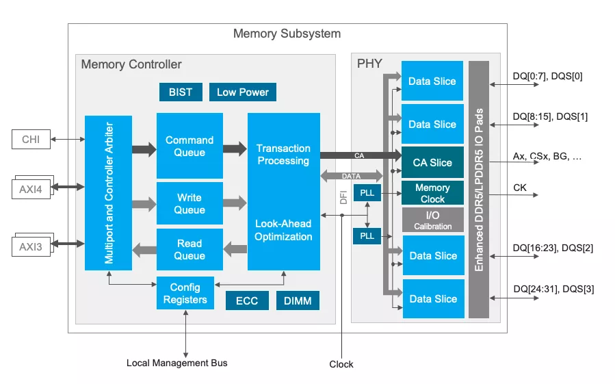
Block Diagram

Benefits

  • Multi-protocol Solution: DDR and LPDDR supported in a single IP
  • Highly Configurable: Application-specific parameters and floorplan optimization
  • Low Power and Area: Industry-leading PPA based on advanced architecture and implementation
  • Low Latency: For data-intensive applications
  • Reliable: Maximum system margin with advanced clocking and I/O architectures
  • Future proof: Cutting edge technology with the latest GDDR protocols and the highest data rates

Applications

  • Data Processing

What’s Included?

  • Clean, readable, synthesizeable Verilog RTL
  • Synthesis and STA scripts
  • Documentation—integration and user guide, release notes
  • Sample verification testbench with integrated BFM and monitors

Specifications

Identity

Part Number
DDR/LPDDR PHY and Controller
Vendor
Cadence Design Systems, Inc.
Type
Silicon IP
Controller / PHY
Controller

Files

Note: some files may require an NDA depending on provider policy.

Provider

Learn more about DDR IP core

DFI 6.0 Key Highlights of the Latest DFI Specification

DFI 6.0.1 (also referred to as DFI 6.0 in the rest of the blog) is the latest standard of the DFI specification. It removes support for earlier DDR/LPDDR generations, adds support for LPDDR6 and HBM4, adds/modifies low-power features, reorganizes WCK and memory-error handling, removes the disconnect protocol, and adds support for 1:3 and 1:6 DFI ratios.

SOCAMM: Modernizing Data Center Memory with LPDDR6/5X

Small Outline Compression-Attached Memory Module (SOCAMM) has made its way into the data center as an alternative to external CPU memory, due to its high performance, low power, memory capacity, and scalability.

Heterogeneous Multicore using Cadence IP

This blog presents a heterogeneous multicore system built with the RISC-V Host CPU and Cadence IP: Xtensa DSPs, and the Janus Network-on-Chip (NoC). While this example uses an RISC-V CPU, any other ISA with similar capabilities can also serve as the host CPU.

The Power of Shifting Left: Cadence Accelerating Innovation with Arm

In semiconductor design, projects are remembered for their extremes—legendary successes and cautionary failures. The difference often hinges on when problems are discovered. A bug found late in development can derail timelines and budgets. This is why "shifting left"—moving testing and validation earlier in the process—is now a critical strategy for innovation.

Boosting AI Performance with CXL

AI workloads are outpacing traditional memory architectures—but CXL®︎ offers a smarter path forward. Cadence's blog, "Boosting AI Performance with CXL," outlines how CXL enables dynamic memory expansion, memory sharing, and maintains coherency across devices to eliminate bottlenecks and boost performance for processing training and inference in large-scale AI systems.

Cadence Drives Next-Gen Memory and Connectivity at FMS 2025

Cadence continues to invest significant engineering effort to deliver advanced, user-friendly IP solutions across a range of essential protocols, two of which were on display at the recent Future of Memory and Storage (FMS) conference in Santa Clara, CA.

Frequently asked questions about DDR Interface IP

What is DDR/LPDDR PHY and Controller?

DDR/LPDDR PHY and Controller is a DDR IP core from Cadence Design Systems, Inc. listed on Semi IP Hub.

How should engineers evaluate this DDR?

Engineers should review the overview, key features, supported foundries and nodes, maturity, deliverables, and provider information before shortlisting this DDR IP.

Can this semiconductor IP be compared with similar products?

Yes. Buyers can compare this product with similar semiconductor IP cores or IP families based on category, provider, process options, and structured technical specifications.

×
Semiconductor IP