Ensuring reliability in Advanced IC design

Siemens EDA and Sofics Webinar 2025
Introduction
To complete our task as engineers we rely on the tools we use. We collaborated with Siemens EDA solutions back in 2025 on a webinar about how we use their tools to develop our designs and layouts.
In this webinar, which is available here https://www.eda-solutions.com/resources/ensuring-reliability-in-advanced-ic-design-webinar/, Khalid presented how the Siemens EDA tools can support chip designers, including simulation, layout and schematic for both analog, digital and mixed signal design flows. Wouter from Sofics talked about how we detect and solve Safe Operating Area violations (SOA) in over-voltage tolerant (OVT) designs. Read more about OVT I/Os in this article Types of overvoltage tolerant I/O. In the webinar we discussed what these problems are, how they arise and the approach we use not only to solve them in this specific example, but also to implement such solutions in our overall design flow.
Webinar overview
In this webinar, Siemens first provide an overview of their EDA ecosystem and how it supports the full IC design flow from schematic and simulation to layout and verification. This includes both analog and digital design environments, as well as mixed-signal integration. The combination enables designers to work across different domains within a single connected flow.
The webinar also highlights key tools such as their simulation environment and Calibre for physical verification, showing how they contribute to improving design accuracy, scalability and reliability. Particular attention is given to how these tools help address challenges related to advanced technology nodes and increasing design complexity.
This overview sets the context for how the tools are applied in practice and how they support a structured and efficient design methodology, which is then demonstrated through a concrete Sofics design example.
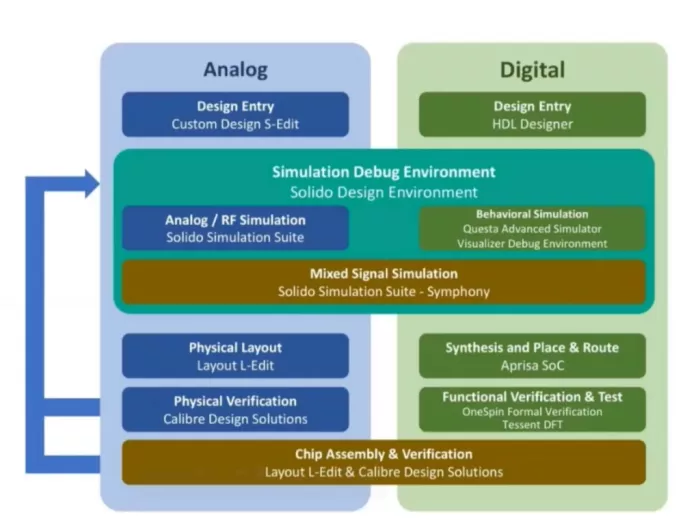
Figure 1. Siemens EDA design flow chart.
Siemens EDA design flow overview
Instead of having stand alone tools, Siemens EDA offers a more complete ecosystem for IC design. It is an integrated design flow that supports the full development cycle, from schematic capture through to final sign-off and manufacturing. What stands out is not just the individual tools, but the overall flow they aim to support. Siemens EDA describes a solution-based ecosystem that spans schematic, simulation, layout, and sign-off verification. The tools are not a single environment, but the intent is clear to reduce friction between steps and keep results traceable across the flow.
In practice, this reduces manual effort and avoids common issues between steps. Mismatches are less likely and problems can be identified earlier, when they are still easy to resolve. This becomes increasingly important in advanced nodes, where small inconsistencies can have a large impact. The benefit is therefore not only access to strong tools, but a more consistent way of working. It allows designers to move forward with greater confidence that what is simulated and verified will carry through to the silicon and final product.
Over-voltage tolerant GPIO design and SOA issues
Wouter’s (Sofics) topic was over-voltage tolerant GPIOs. These are I/Os that can handle a pad voltage that is higher than what the devices in an advanced node can safely see. But why would you want to go beyond the limits of a technology? The reason is simple. In a modern node, an I/O device might be limited to around 1.8V. However, this advanced chip needs to communicate to older components in the system still running on 3.3V. That higher voltage shows up at the GPIO pad.
An overvoltage tolerant GPIO still looks familiar at block level: driver, receiver, pull resistance, ESD protection… The difference is what happens inside when the pad goes above the device limit. The key reliability concept is called safe operating area (SOA): the current and voltage conditions over which a device can be expected to operate without self-damage or degradation.
This SOA needs to be analyzed both in DC as well as in transient. A design can look fine in DC and still violate SOA during switching. Parasitic capacitances and routing resistance change the timing, especially in advanced nodes. This can create short spikes on internal nodes and trigger SOA violations. That is why checking parasitics matters. The violation often show up in short time periods where voltages do not divide cleanly, stressing the device and degrading the lifetime of the circuit.
OVT design is mainly about controlling those internal voltages. One part of the story is limiting what the pre-driver sees, often by using an intermediate supply node – here called Vm. Another part is keeping the output devices safe by sharing the pad voltage across a stack. Both of these techniques are shown in figure 2. The usage of an intermediate node also means you need a voltage regulator that stays valid across corners and modes. If the regulator’s voltage shifts, this will result in device stress.
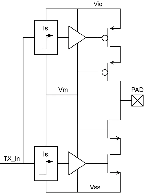
Figure 2. Shows how an intermediate node (Vm) limits pre-driver stress, while stacked output devices share the pad voltage to protect against overvoltage.
The GPIO design cannot be treated separately from the ESD protection: the protection network sits on the same pad. It affects leakage, clamping and internal node behavior. So the OVT strategy has to be compatible with the ESD approach from the start. Therefore special ESD protection is required. Catching SOA issues early is crucial. If you only see them at the end, this means a lot of rework. The solution is including parasitics sooner, running corners as a habit and checking SOA violations with simulation in a repeatable manner.
This is where automation becomes essential. With OVT the number of checks grows quickly, especially when you include corner runs and different operating modes. We use Tcl scripts to standardize how we launch simulations, apply SOA checks and collect results. This flow can be reused across designs with minimal rework. We also keep the output clean with custom filters, so real violations stand out.
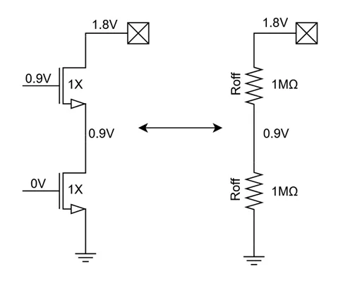
Figure 3. Schematic example of stacking two 0.9V transistors with the voltage over the nodes.
Stacking is a good example of why this approach is needed, shown in figure 3. On paper it looks simple. You split the pad voltage across multiple devices so no single transistor sees too much stress. In practice, the result depends heavily on sizing as seen in figure 4. If the devices do not share the voltage evenly, one device can end up taking most of it. That is where SOA violations show up in DC. In transient there are additional tradeoffs, especially once parasitics are included.
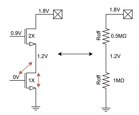
Figure 4. Displays the schematic of a simple 2 stack with size difference between the two transistors and the voltage drop.
In a stacked output, the effective Roff is not a fixed property. It shifts with process and temperature and it depends on biasing and on how the internal stack nodes move during switching. If the devices do not share voltage evenly, one device can see higher stress even when the overall drive strength looks fine. That is why we look at Ron and SOA together under real transitions and with parasitics included.
Layout
The next topic is layout with a focus on FinFET nodes. One important point is that a single GPIO does not follow one fixed layout approach. Instead it combines different styles within the same I/O. Some parts are closer to digital layout and resemble working with standard cells, with an example shown in figure 5. Others behave more like analog or mixed-signal blocks, where layout dependent effects are more important. There are also fully custom regions, especially around ESD, where current handling and robustness drive the layout.
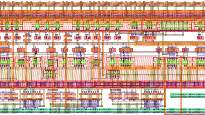
Figure 5. Example schematic and layout views of a GPIO. The figure highlights the standard-cell style blocks and more custom layout used in the same I/O.
Once layout is in place the remaining work is making sure the real implementation still meets the same reliability intent. After layout the full verification flow is applied. This includes DRC with requirements like dummy fill and metal coloring. It also includes LVS with parasitic-aware checks like well-diodes and custom rules where needed. XRC extraction is then used to loop back to the design simulation. On top of that reliability checks such as PERC can be used to confirm ESD implementation. This link between extraction and simulation is also a key theme in our upcoming webinar with Siemens EDA and EDA Solutions this June (2026). We will share two recent design cases where Solido and Calibre xRC helped expose layout-driven effects early enough to improve the final implementation.
Conclusion
Reliability in advanced IC design is not something you “check at the end.” it has to be part of the flow.
Many EDA platforms can connect schematic and layout. The red line in this webinar is using that integration to make reliability checks repeatable during design. Khalid from Siemens EDA showed the connected environment and how simulation and verification stay aligned across the flow. Sofics’ Wouter then showed why it matters in a real world example with OVT GPIOs. Where SOA violations show up during switching, with parasitics, corners, and the ESD sitting on the same pad. Once you extract parasitics you also pull in real layout effects like well and substrate diodes and resistive paths, which can shift internal node behavior and create short stress spikes. When these checks are easy to rerun reliability stops being a surprise at the end of a development cycle.
Q&A
After the main presentation the discussion moved into questions from the audience. These focused on how the flow works in practice, how portable it is across nodes and where the OVT edge cases show up.
The first question was regarding PDK support by Siemens EDA for different foundries and nodes. Siemens EDA confirmed support for FinFET processes such as TSMC 16nm and emphasized that the flow is qualified down to advanced nodes. Related questions came up around enablement and installation details, where topics like metal coloring were mentioned as something that needs to be set up correctly at the technology level, but then runs smoothly once in place.
A second theme was tool integration and modularity. The flow was described as tightly integrated, with tools able to call each other directly from the interface and with back-annotation of results. At the same time it is modular. Users do not need to adopt the full tool chain at once and can pick pieces of the flow as needed.
The Q&A also covered data and format interoperability. Siemens EDA noted support for industry-standard formats such as OpenAccess, OASIS and GDSII and the ability to read design data from other tools into the flow.
From the Sofics side, several questions went deeper into SOA issues in transient behavior. Beyond the examples in the main talk it was confirmed that additional SOA risks appear on both rising and falling edges. One falling-edge case described the mid-node voltage dropping faster than the pad because of smaller capacitive loads and stronger switching in the driver, which you can read more in depth here: Typical SOA violations in a stacked driver. A rising-edge case described the mid-node becoming floating and then being pulled upward through parasitic source drain capacitances, potentially beyond the SOA limit. These cases can lead to conflicting sizing directions and in some situations require a different architecture.
There were also practical questions about how early parasitics are included in schematic design. The answer was: before extraction, because xRC extraction can only be done once the layout is ready. The main examples were expected well diodes, which can become significant once forward biased even if it’s small in size. Parasitic capacitances can also be estimated early, but sizing them is more difficult and often comes down to experience and best-guess values.
Intermediate voltage supply generation came up as well. An LDO implementation for Vm generation was described as typical, but alternatives were also mentioned. One issue with an LDO is that it is not good at handling current pushed back into the rail. A second issue is that these voltage regulors are major power consumers and always need to stay active to protect the I/Os. They are often shared across multiple I/O cells to reduce the power and area consumption. A rough estimate is 60μA to 100μA steady-state current per voltage regulator, which is why Sofics is developing topologies that reduce this toward the low microamp to even nanoamp range.
Finally, questions returned to automation and portability. Tcl scripting was discussed both as a way to configure device sizing and conventions and as a practical way to port designs between technology nodes when working in OpenAccess-based environments. Siemens EDA also noted that S-Edit exposes a Tcl API that supports instance manipulation and connectivity, which makes these scripted flows easier to build and reuse.
Explore ESD Protection IP:
- On-chip ESD/EOS/Latch up/EMC protection for high voltage and BCD processes
- Robust circuit and interface solutions
- On-chip ESD/EOS/Latch up protection for advanced and low voltage processes
Related Semiconductor IP
- On-chip ESD/EOS/Latch up/EMC protection for high voltage and BCD processes
- Robust circuit and interface solutions
- On-chip ESD/EOS/Latch up protection for advanced and low voltage processes
- ESD Protection
- High-Speed 3.3V I/O library with 8kV ESD Protection in TSPCo 65nm
Related Blogs
- Applied AI in Analog IC Design Migration
- 2025 Year in Review: Design Wins, Advanced Nodes, and Expanding Markets
- Bulletproofing PCIe-based SoCs with Advanced Reliability, Availability, Serviceability (RAS) Mechanisms
- Don't Let the Bugs Bite: Reducing Design Reworks and Errors with Advanced Linting (Part 1)
Latest Blogs
- Ensuring reliability in Advanced IC design
- A Closer Look at proteanTecs Health and Performance Management Solutions Portfolio
- Enabling Memory Choice for Modern AI Systems: Tenstorrent and Rambus Deliver Flexible, Power-Efficient Solutions
- Verification Sanity in Chiplets & Edge AI: Avoid the “Second Design” Trap
- Embedded Security explained: Cryptographic Hash Functions