Understanding the Power Consumption of Modern High Bandwidth Memory: Experimental Analysis and Modeling Using Real HBM2 DRAM Chips
By Ataberk Olgun 1, Spiros Galanopoulos 1, Andreas Kosmas Kakolyris 1, İsmail Emir Yüksel 1, Haocong Luo 1, F. Nisa Bostancı 1, Onur Mutlu 1, 2
1 ETH Zurich
2 New York University
Abstract
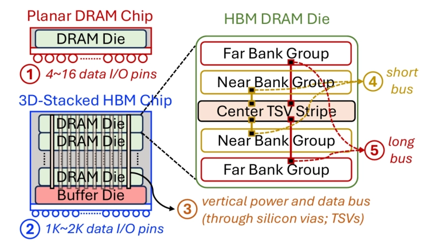
We perform the first comprehensive experimental characterization of power consumed by real HBM2 DRAM chips. Our extensive characterization of 36 HBM2 chips yields 1) the empirical basis for developing new, accurate HBM power models or validating existing power models and 2) key insights into structural and data-pattern-dependent variation of power in HBM2 chips. Out of our 13 new findings and 6 key takeaway messages, we highlight: 1) a read operation consumes higher current than any other tested operation including refresh (by 3.1 ×), 2) HBM2 read current significantly varies across bank groups (by 8.1%) and banks (by 5.3%), and 3) the toggled data bus signals in a data transfer burst significantly affect current draw. For example, toggling all HBM2-internal bank group bus signals causes 29.4% higher power consumption than keeping them constant. Leveraging our empirical insights into HBM2 power consumption, we carefully engineer an access pattern that yields 23.6% (35.4%) higher power consumption on average (maximum) across all tested HBM2 chips than the highest-power-consuming JEDEC-specified current measurement loop.
Our results have important implications for HBM-based system design and validation. For example, relying solely on JEDEC- or vendor-specified test loops to bound HBM power could cause errors or system failures, thermal throttling, and thermal shut downs in real-world high-power, high-performance computing or AI/ML workloads. To improve3D-stacked DRAM power modeling fidelity in open source architectural simulation infrastructures, we develop a new HBM power model, guided by our characterization and built on DRAMPower, that captures structural and data-pattern-dependent power variation. Our model predicts the power of 36 real HBM2 chips across diverse workloads (including a real LLM decode workload) with 7.6–8.1% mean absolute percentage error, substantially more accurately than state-of-the-art HBM power models (which have error between 20–42%). We validate our model against real HBM3E GPU memory power consumption. The power consumption predicted by our model for a power-intensive microbenchmark closely matches (with 2.4% to 5.3% error across HBM3E’s specified supply voltage range) the average memory power consumed by three tested NVIDIA H200 GPUs. We use the power model to project the read energy of future HBM4 chips. We publicly release our power model at https://github.com/CMU-SAFARI/HBM-Power.
To read the full article, click here
Related Semiconductor IP
- HBM Memory Model
- HBM DFI Verification IP
- HBM 4 Verification IP
- HBM Synthesizable Transactor
- HBM DFI Synthesizable Transactor
Related Articles
- High bandwidth memory (HBM) PHY IP verification
- Design Considerations for High Bandwidth Memory Controller
- High Bandwidth Memory (HBM) Model & Verification IP Implementation - Beginner's guide
- TeraPool: A Physical Design Aware, 1024 RISC-V Cores Shared-L1-Memory Scaled-up Cluster Design with High Bandwidth Main Memory Link
Latest Articles
- The Era of Vibe Tapeout: Dark Age or Golden Age for Analog Circuit Design?
- Understanding the Power Consumption of Modern High Bandwidth Memory: Experimental Analysis and Modeling Using Real HBM2 DRAM Chips
- BARE-AI: Bit-Flip Attack Resilience in AI Hardware through Built-in Performance Monitors
- RFChipAgent: Multi-Agentic AI Flow for Analog/RF Chip Design
- Anechoic: Onsager-Corrected Parallel Annealing for Sub-0.1 ms Dense Max-Cut on an FPGA