Novel Spare Cell Architecture
Shailesh Kumar, Rahul Saxena, Vikas Garg, Piyush Kumar Mishra (Freescale Semiconductors)
Introduction
Systems on Chip (SoC) are required to go through revisions for various reasons. The wisdom lies in proper planning to accommodate these revisions. An intelligent way is to implement the revision in metal layers only while avoiding any base layer changes because base layer changes are much more costly than metal layer changes.
These revisions generally referred as Engineering Change Orders (ECO) are implemented by adding spare cells (i.e., additional stdcells and flip-flops) across the SoC. These spare cells have their inputs tied and outputs floating. The cells lie idle doing nothing unless needed to implement an ECO. If required their connectivity is changed to attain the functionality specified by the ECO. This change in connectivity is done through changes in metal layers. Thus, the addition of cells (base change) can be avoided and the ECO is implemented through a relatively less expensive metal only change.
This technique is good for limiting the impact of changes but has its own limitations, which are that the required cells must lie in close proximity to the section of the physical logic being revised. If the required cell is placed very far away, then constraints like routability and timing could render that cell useless. An alternative is to place as many spare cells as possible. Hypothetically, all the space left after regular placement is a candidate for a spare cell but this would mean no place for decoupling capacitors (decaps), which are required for dynamic performance of the SoC. The decaps are necessary to smoothen the power profile by feeding the local surge of current during switching of stdcells.
We propose modifying the spare cell into a cell that acts like a decap yet could be converted into a working stdcell through a metal only change if a revision is required. Thus, we add as many modified spare cell as possible that act like decaps and when required use them functionally through a metal layer change.
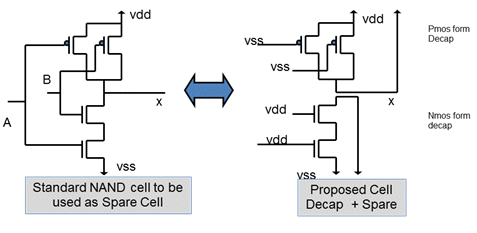
Schematic diagrams of a spare cell and our proposed spare cell are shown in FIG. 1. Although this spare cell is for an inverter, it is applicable to all kind of stdcells.
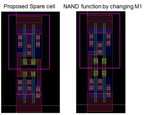
Note the break in POLY as compared to the regular cell where it is continuous. Here, we would add the modified spare cell that would act as decap but if required could be changed to a regular cell through a Metal 1 change.
This would improve the possibility of locating a spare cell in close proximity to the changed logic and avoid a base layer change. There is little change required to the normal Place and Route flow, shown below.
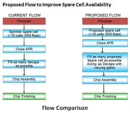
With the proposed flow, the availability of the spare cell has increased considerably. This can help avoid situations where non-availibility of enough and appropropriate cells in the proximity warrants a costlier base layer change. With proposed flow, the change could be implemented as metal ECO only. Secondly, the spare cells would be used as DECAPs if not being used functionally.
** The new method can drastically improve the availability of spare cells but 100 % ECO coverage can not be claimed.
Details about the authors:
Shailesh Kumar (shailesh.kumar@freescale.com): Working at Freescale Semiconductors, India as Staff Engineer and 7 years of experience in Physical Design.
Rahul Saxena (rahul.saxena@freescale.com): Working at Freescale Semiconductors, India as Principal Staff Engineer and 12 years of experience in Physical Design, Analog Layout Design and Standard Cell Library Design.
Vikas Garg (b00597@freescale.com): Working at Freescale Semiconductors, India as Staff Engineer and 8 years of experience in Physical Design.
Piyush Kumar Mishra (piyush@freescale.com) : Working at Freescale Semiconductors, India as Principal Staff Engineer and 12 years of experience in Physical Design.
Related Semiconductor IP
- nQrux® Root of Trust IP
- AXI to UCIe Bridge IP
- UCIe 2.x Controller IP
- SWI3S (SoundWire I3S Interface) Peripheral Controller Core IP
- OpenTitan-based RISC-V Secure Element
Related Articles
- A Novel Mesh Architecture for On-Chip Networks
- A Standard cell architecture to deal with signal integrity issues in deep submicron technologies
- Forward-Looking SoC-based PHY Architecture for Macro and Small Cell LTE eNode-Bs
- Reconfiguring Design -> C-based architecture assembly supports custom design
Latest Articles
- A Secure dToF LiDAR SoC with Dual-Domain Fingerprinting and Event-Driven AFE Circuit Achieving Sensor-Level Attack Resilience
- ZTA-Q: an Open-source RISC-V Platform for Accurate Quantized CNN Inference
- Automated Pre-Silicon Verification of High-Speed DDR5 and LPDDR5/6 Memory Controllers: Closed-Loop Timing, Mode Register, and PHY Synchronization in UVM
- U-Sonic: An Open-Source 8-Channel Ultrasound Transmit IP in a 130 nm RISC-V SoC
- S-ALSA: Co-Design of Adiabatic Logic-based Sensing and Balanced Bit-Cells for Secure and Energy-Efficient MRAM