Hardware Acceleration of Kolmogorov-Arnold Network (KAN) in Large-Scale Systems
By Wei-Hsing Huang 1, Jianwei Jia 1, Yuyao Kong 1, Faaiq Waqar 1, Tai-Hao Wen 2, Meng-Fan Chang 2,3, Shimeng Yu 1
1 School of Electrical and Computer Engineering, Georgia Institute of Technology
2 Department of Electrical Engineering, National Tsing Hua University (NTHU)
3 Taiwan Semiconductor Manufacturing Company (TSMC)
Abstract
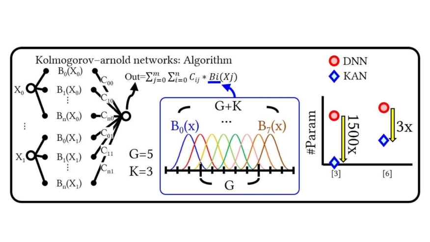
Recent developments have introduced Kolmogorov-Arnold Networks (KAN), an innovative architectural paradigm capable of replicating conventional deep neural network (DNN) capabilities while utilizing significantly reduced parameter counts through the employment of parameterized B-spline functions with trainable coefficients. Nevertheless, the B-spline functional components inherent to KAN architectures introduce distinct hardware acceleration complexities. While B-spline function evaluation can be accomplished through look-up table (LUT) implementations that directly encode functional mappings, thus minimizing computational overhead, such approaches continue to demand considerable circuit infrastructure, including LUTs, multiplexers, decoders, and related components. This work presents an algorithm-hardware co-design approach for KAN acceleration. At the algorithmic level, techniques include Alignment-Symmetry and PowerGap KAN hardware aware quantization, KAN sparsity aware mapping strategy, and circuit-level techniques include N:1 Time Modulation Dynamic Voltage input generator with analog-compute-in-memory (ACIM) circuits. This work conducts evaluations on large-scale KAN networks to validate the proposed methodologies. Non-ideality factors, including partial sum deviations from process variations, have been evaluated with statistics measured from the TSMC 22nm RRAM-ACIM prototype chips. Utilizing optimally determined KAN hyperparameters in conjunction with circuit optimizations fabricated at the 22nm technology node, despite the parameter count for large-scale tasks in this work increasing by 500Kx to 807Kx compared to tiny-scale tasks in previous work, the area overhead increases by only 28Kx to 41Kx, with power consumption rising by merely 51x to 94x, while accuracy degradation remains minimal at 0.11% to 0.23%, demonstrating the scaling potential of our proposed architecture.
To read the full article, click here
Related Semiconductor IP
- DSP-Based 112G SerDes
- XTAL oscillator in TSMC-7nm
- GPU
- V-by-One Verification IP
- AI model compression IP
Related Articles
- Role of Embedded Systems and its future in Industrial Automation
- The Growing Imperative Of Hardware Security Assurance In IP And SoC Design
- Hardware vs. Software Implementation of Warp-Level Features in Vortex RISC-V GPU
- From I2C to I3C: Evolution of Two-Wire Communication in Embedded Systems
Latest Articles
- SEAM-V: A Hybrid-Decoupled RISC-V Vector Processor with Backend-Visible EP Context for Sustained Vector Throughput
- New Number Formats for FFT IP Cores in Optical OFDM Transceivers
- Reducing Power Consumption of Embedded Dynamic Memories with ECCs
- NIFA: Nonlinear IMC enhanced FPGA for efficient ML inference
- A 32-channel event-based bio-signal analog front-end with adaptive delta and pulse frequency encoding