Fully-programmable SoCs -- A new breed of devices
Dr. Syed Ijlal Ali Shah, Arteris
November 11, 2016 (embedded.com)
Generally, silicon devices that process information can be classified as being either SoCs, ASICs/ASSPs, or FPGAs (System on Chip, Application-Specific Standard Parts, Application-Specific Integrated Circuits, and Field-Programmable Gate Array components). It is very difficult to perform power, performance, and cost comparisons between these technologies without looking at specific applications and running benchmarks. However, it may be possible to take an application and map it to comparable devices in the three categories. If we were to do so, we would probably come up with a table like the one below.
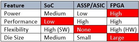
Figure 1. High-level comparison of devices (Source: Dr. Shah)
It is evident from this table that each device category has its own strengths and weaknesses.
ASICs/ASSPs, SoCs & FPAGs: A brief description
ASICs/ASSPs are built to perform very specific functions efficiently, and -- as such -- are optimized in terms of performance, power, and cost. They offer the smallest die size and lowest power consumption, and they may have the best performance-to-power ratio. However, ASICs/ASSPs do not offer any flexibility; that is, once the device has been fabricated, it can only perform the specific function for which it was designed and nothing else. As such, ASICs/ASSPs are developed for applications or functions that have matured or are standardized with no requirement for change in the future. Since ASICs/ASSPs are built to perform very specific functions, from an ROI (return on investment) perspective, they make sense only when the volumes are large as so to be able to recoup their substantial development costs.
To read the full article, click here
Related Semiconductor IP
- FlexGen Multi-Die Smart Network-on-Chip (NoC) IP
- FlexGen Smart Network-on-Chip (NoC) IP
- FlexWay Interconnect IP
- Ncore Multi-Die Interconnect IP
- Magillem Registers
Related Articles
- Terracotta: Enabling the Adoption of New DRAM Techniques via a Flexible DRAM Interface and Memory Controller
- Growing demand for high-speed data in consumer devices gives rise to new generation of low-end FPGAs
- A new era of chip-level DRC debug: Fast, scalable and AI-driven
- VitaLLM: A Versatile and Tiny Accelerator for Mixed-Precision LLM Inference on Edge Devices
Latest Articles
- Automated Multi-Line Bug Repair Using Model Checker Aided LLMs: A Case Study on RISC-V Processors
- Cryogenic Recharacterization of a Commercial 22 nm FD-SOI Foundry Standard-Cell Library
- A 105 MS/s 4.18 nJ/inference 0.765 mm² Mixed-Signal Streaming ML Engine for Wireless Baseband in 12LP+ FinFET
- Agentic AI for Heterogeneous System Design Across Chip, Scale-Up, and Scale-Out Domains
- Minimum RISC-V: Maximum FPGA Efficiency