The Fastest Path to Scalable Photonic Systems: Using Proven IP for both PIC and EIC designs

Why photonic system designers should (re)use validated IP on both sides of the optical-electrical interface
Artificial Intelligence infrastructure is driving an enormous increase in the amount of data that must move between processors, accelerators and memory. As conventional electrical interconnects face increasing challenges in bandwidth, reach and power consumption, photonics are becoming an important part of the solution. Every day new articles are published discussing how photonics can break through the memory wall.
Most practical photonic systems combine a Photonic Integrated Circuit (PIC), which manipulates photons, with an Electronic Integrated Circuit (EIC) that manipulates electrons.
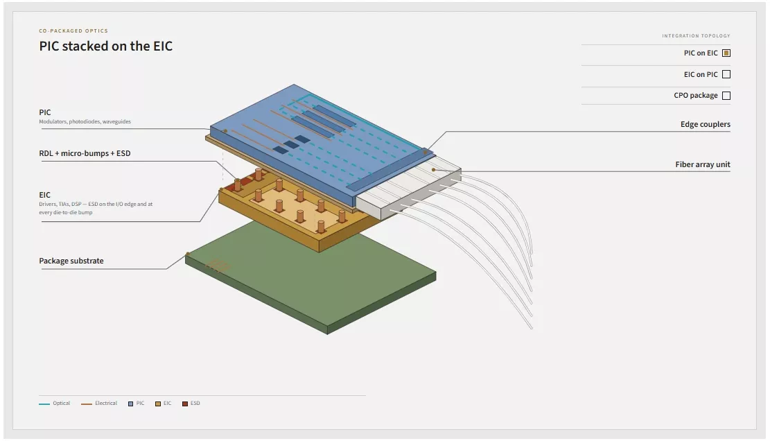
Both types of chips require highly specialized design expertise and dedicated manufacturing processes. Both must also ultimately work together seamlessly. And both can take considerable time and engineering effort to develop from scratch.
The best approach for such a design task is to start from proven IP on both sides. Alcyon Photonics and Sofics bring complementary expertise to this challenge. Alcyon provides validated photonic building blocks and PIC design expertise, while Sofics provides silicon-proven specialty I/O and ESD protection IP for the electronic IC. The objective is the same on both sides: reduce development risk, shorten design cycles, scale with confidence and allow customers to concentrate their engineering resources on the features that truly differentiate their product. This complementary approach is the foundation of the partnership announced by Alcyon Photonics and Sofics in April 2026.
Do not reinvent the building blocks
Developing a new semiconductor product always involves a trade-off between differentiation and reuse. Some circuits are fundamental to the value of the product and deserve significant internal engineering effort. Others are necessary building blocks: they must perform correctly, integrate smoothly with the rest of the design and be manufacturable, but designing them again from the ground up provides little competitive advantage. The same balance between differentiation and reuse applies to both the PIC and the EIC.
Validated IP on the PIC side
On the photonic side, designers need functions such as wavelength multiplexers, directional couplers and multimode interferometers.
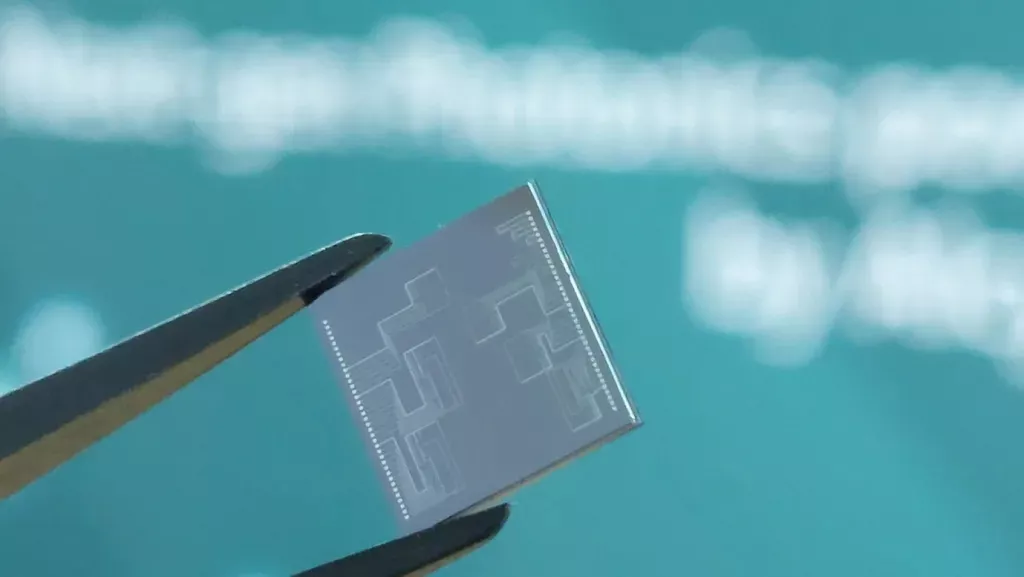
Leveraging proven IP and design ecosystems reduces development risk, shortens design cycles and accelerates time-to-market. Alcyon Photonics supports this reuse strategy through validated photonic IP libraries and a comprehensive design environment that helps bridge the gap between simulation and high-volume manufacturing.
By starting from validated building blocks rather than developing every photonic function from scratch, development teams can reduce design iterations and move more confidently from simulation toward fabrication and volume manufacturing.
Alcyon Photonics delivers validated, fabrication-ready integrated photonic IP designs engineered for performance and reliability on silicon photonics, Indium Phosphide and Thin-Film Lithium Niobate among the supported material systems. The comprehensive IP libraries of proven architectures, combined with advanced design, simulation, and layout services, integrate seamlessly with leading foundries to reduce development time and improve yield.
With deep expertise in high-speed, low-power photonic engineering, Alcyon Photonics enables robust solutions that scale reliably from prototype to volume production.
The EIC–PIC interface is not a standard GPIO
The same reuse strategy applies on the EIC side: designers can start from proven IP, but that IP still needs to be suited to the application. This distinction is particularly important at the interface between the EIC and PIC. These interfaces have requirements that are very different from conventional chip I/O. A conventional, general-purpose I/O cell is not necessarily a good starting point. Its ESD protection may contribute too much capacitance, its physical footprint may be unnecessarily large, and its voltage or drive capability may not match the photonic interface.
These interface-specific requirements make specialty I/O and application-specific ESD protection part of the design rather than an afterthought.
Not every interface needs the same ESD protection
The required ESD robustness depends on where an interface is used. A pin exposed to board-level handling and assembly typically requires standard component-level ESD protection. An interface connecting two bare dies inside the same package operates in a very different environment. Applying the same ESD target to both leads to unnecessary protection overhead.
For example, traditional general purpose I/O (GPIO) protection can be designed for HBM robustness above 2 kV, whereas a co-packaged EIC–PIC interface may only require a fraction of that robustness. The important point is not simply to reduce ESD protection. It is to select the appropriate protection level for each interface, based on its actual handling, assembly and operating environment.
Reducing the required ESD level can create a valuable design trade-off: less ESD robustness where the application allows it can mean lower capacitance and smaller area which will lead to higher performance.
Low-capacitance protection for high-bandwidth interfaces
Traditional ESD protection structures used in GPIOs become a significant part of the capacitance budget of a high-bandwidth interface. For sensitive receiver inputs and high-speed EIC–PIC connections, that parasitic load directly compromises the performance. Sofics therefore developed low-capacitance ESD protection specifically for high-speed interfaces.
Low-capacitance protection is especially relevant for AI and data-center applications, where bandwidth density and energy efficiency are critical. Sofics has already been involved in more than 40 data-center-related projects, including work for AI training, CPU/GPU and optical-communication applications.
The right I/O for the right voltage
Photonic EICs also require voltage levels that do not always align naturally with the transistor options available in advanced CMOS processes. A modulator driver, for example, typically requires a larger voltage swing or bias than a standard interface in the same technology. Conversely, other interfaces operate at 1 V or below while demanding extremely low capacitance. Matching these different interface requirements becomes increasingly important as photonic systems move to advanced CMOS. Sofics has worked on photonics-related interfaces across advanced technologies ranging from CMOS and FinFET processes to 2 nm nanosheet technology.
Rather than adapting the photonic architecture to whatever standard I/O happens to be available, the electrical interface can therefore be optimized for the application.
Designed for the foundry ecosystem
Reusable IP only creates real value when it can be implemented in the manufacturing technology selected for the product.
Foundry compatibility is another area where the complementary capabilities of Alcyon and Sofics are valuable. Both companies work with established semiconductor foundries and technology platforms.
Alcyon’s photonic IP is developed around supported photonic foundry platforms. Sofics similarly develops its specialty I/O and ESD solutions within the target CMOS process and qualification environment.
Foundry partnerships from Alcyon Photonics for PIC circuits
Foundry partnerships from Sofics for EIC circuits
Working within established foundry platforms helps move development away from isolated custom blocks toward a repeatable design methodology compatible with established foundry flows.
Conclusion: Two chips. One system. One development challenge.
As photonics move into AI infrastructure, co-packaged optics, high-performance computing, sensing and other volume applications, the challenge is no longer simply to demonstrate an innovative optical function. The complete system must deliver performance, reliability and manufacturability, at scale. That requires both sides of the system to work.
Alcyon Photonics brings proven photonic IP and design expertise to the PIC. Sofics brings specialty I/O and ESD protection IP to the EIC. Together, the companies give development teams access to established building blocks and specialized expertise across the electrical–photonic boundary.
The philosophy is straightforward:
- Reuse what is already proven.
- Optimize what needs to be different.
- Focus your engineering effort on what makes your product unique.
- For companies developing the next generation of photonic systems, that can mean fewer design iterations, lower technical risk and a faster route from concept to silicon and ultimately to volume production.
Related Semiconductor IP
- On-chip ESD/EOS/Latch up/EMC protection for high voltage and BCD processes
- Robust circuit and interface solutions
- On-chip ESD/EOS/Latch up protection for advanced and low voltage processes
- TSMC 40nm 5V GPIO
- TSMC 22nm 1.0V, 1.2V & 1.8V GPIO
Related Blogs
- Breaking the Bandwidth Barrier: Enabling Celestial AI’s Photonic Fabric™ with Custom ESD IP on TSMC’s 5nm Platform
- Unveiling Ultra-Compact MACsec IP Core with optimized Flexible Crypto Block for 5X Size Reduction and Unmatched Efficiency from Comcores
- Meeting the World's Growing Bandwidth Demands with a Complete 1.6T Ethernet IP Solution
- Industry's First Verification IP for Arm AMBA CHI-G
Latest Blogs
- The Fastest Path to Scalable Photonic Systems: Using Proven IP for both PIC and EIC designs
- Building Trusted AI Agents from the Silicon Root of Trust
- Heterogeneous Computing in Space
- BEVFormer-Tiny on Chimera: Bird's-Eye-View Perception in One GPNPU Kernel
- PUF vs. HSM? Why It's Not Either/Or for IoT Compliance