Engineering FPGA Products: Moving Beyond RTL

Designing an FPGA-based product can look straightforward when working within the FPGA development environment. But the design also has to work reliably with the board, processor, memory, firmware, drivers, and application software.
The real challenge lies when the design moves from development and simulation to the actual product hardware.
The transition from an evaluation platform to a production-ready product often exposes issues that are difficult to see during RTL development. DDR behaviour can change with the PCB layout and signal integrity. PCIe performance can change under sustained traffic. Processor boot can depend on power sequencing, while software bring-up depends on the interfaces between the FPGA and processor.
The system can also meet its functional requirements and still fall short on latency, power, or thermal limits. These issues are not necessarily failures of the FPGA design itself. They result from how the different parts of the product interact.
This is why FPGA engineering extends beyond RTL. Hardware, programmable fabric, processor, firmware, drivers, and software have to be designed and validated as parts of the same system.
The FPGA Is the Practical Bridge Between a Module and Custom Silicon
An FPGA sits between a ready-made hardware platform and custom silicon.
A System-on-Module (SoM) provides a starting point with several components already integrated. An ASIC is designed for a specific function and can provide higher efficiency and performance at volume, but requires significant investment in architecture, verification, manufacturing, and validation. A silicon respin may be required when a post-fabrication change cannot be addressed through other means.
An FPGA provides programmable hardware between these two approaches. Its functionality can be changed as the product requirements evolve, without changing the underlying silicon.
Where FPGA Fits
FPGAs are used for workloads that require parallel processing, high data throughput, predictable timing, or hardware flexibility.
DSP, communication, radar, LiDAR, sonar, and networking workloads can use programmable logic for real-time processing and data-path acceleration.
Re-programmability also allows the hardware to evolve with product requirements. FPGA architecture therefore has to consider compute, memory bandwidth, I/O, latency, power, and thermal limits.
The FPGA Itself Has Changed
FPGAs have moved beyond programmable logic. Modern devices can integrate processors, DSP resources, memory, high-speed interfaces, and acceleration within the same device.
As more functions move into the FPGA, its role in the product also changes. A function implemented in the fabric can affect the board architecture, memory, data paths, firmware, drivers, and system software.
The FPGA is therefore becoming part of the system architecture, not just a programmable component on the board.
Why FPGA Product Engineering Is Needed
This broader role also changes how the product has to be engineered. The work extends beyond RTL.
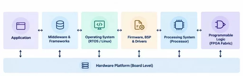
Complete FPGA Product Stack
The hardware/board, programmable fabric, and embedded platform management all have to work together. Power, clocks, memory, interfaces, timing, data movement, and thermal limits have to be considered across the system.
A change in one area can also affect another. An FPGA interface change can require driver changes. A memory architecture change can affect software. A board change can introduce signal integrity or power issues that were not visible during RTL development.
The product therefore has to be validated as a complete system, not only as an FPGA design.
Three Pillars Must Be Engineered Together
An FPGA product brings together three engineering pillars: Hardware Design, Programmable Fabric, and Platform Management, which must be engineered together rather than treated as separate activities.
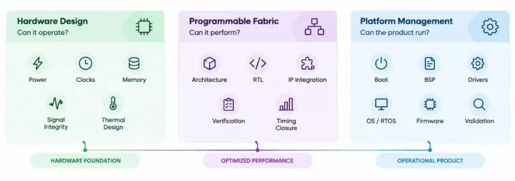
Three Engineering Pillars
- Hardware Design: The hardware provides the physical foundation for the FPGA platform. Power sequencing, clocks, DDR, high-speed interfaces, signal integrity, EMI, and thermal behaviour all affect system reliability. A custom board can also introduce constraints that are not visible on an evaluation platform. The hardware has to support the requirements of the programmable fabric. An FPGA can have sufficient logic resources and still miss the required throughput if memory bandwidth or data movement becomes the bottleneck. Hardware Design therefore has to account for these dependencies from the beginning.
- Programmable Fabric: Programmable Fabric starts with system architecture and moves into RTL design and IP implementation. The architecture defines data paths, interfaces, memory access, and functional partitioning before RTL implementation begins. The design then has to be verified for functionality, timing, resource usage, and performance. A design can pass simulation and fail timing after implementation. It can also meet timing and still expose a data-path or clock-domain issue during system testing. Programmable Fabric therefore covers architecture, RTL, IP integration, DSP or acceleration, verification, timing closure, and resource optimization.
- Platform Management: Platform Management connects the FPGA platform to the software stack. FPGA configuration, firmware, BSP, HAL, drivers, operating system, diagnostics, and updates have to work together for the platform to boot and operate correctly. The processor architecture can vary across platforms, including ARM and RISC-V. Software environments can include Linux, Zephyr, FreeRTOS, and VxWorks. Platform work can include processor bring-up, peripheral drivers, boot software, and application integration. Memory maps, interrupts, buffer ownership, data movement, and cache behaviour also have to be defined between hardware and software. These interfaces become particularly important in multimedia, sensor processing, and AI workloads.
For product teams, FPGA hardware design can span multiple engineering activities, from design through verification, implementation, integration, and product validation. MosChip supports FPGA development from idea to production across leading FPGA platforms, including AMD, Altera, Lattice, and Microchip.
The engineering work includes board design, board bring-up, IP porting, peripheral and interface integration, protocol validation, DSP and vision processing, verification, timing closure, FPGA migration, CPU/SoC integration, hardware acceleration, BSP, middleware development, and FPGA-based reference designs. This helps product teams develop, validate, and evolve FPGA-based products as requirements change.
Related Semiconductor IP
- 100M/1G/ TSN Endpoint DO-254 IP Core
- Image Signal Processor
- H.265 / HEVC Video Codec
- H.264 / AVC Video Encoder
- Crest Factor Reduction
Related Blogs
- The interface makes the FPGA
- Open-Silicon adds Silicon Logic Engineering - for a good reason
- Altera's intros 28nm Stratix V FPGA family
- Xilinx unleashes triad of low-power, 28nm FPGA families with very promising characteristics for memory interfacing