EDA AI Agents: Intelligent Automation in Semiconductor & PCB Design

The next era of semiconductor and PCB design will be defined by two parallel imperatives: making core engines faster and making engineers more productive. On the engine side, the industry is embedding machine learning and reinforcement learning directly into EDA tools — enabling, for example, local models built from a small set of SPICE simulations to dramatically accelerate verification while maintaining near-SPICE accuracy. Simultaneously, leading EDA vendors are partnering with hardware companies such as NVIDIA to GPU-accelerate core algorithms, unlocking vastly higher throughput across simulation, design exploration, coverage analysis, and OPC. Addressing the second imperative of engineering productivity demands a fundamentally different kind of AI solution.
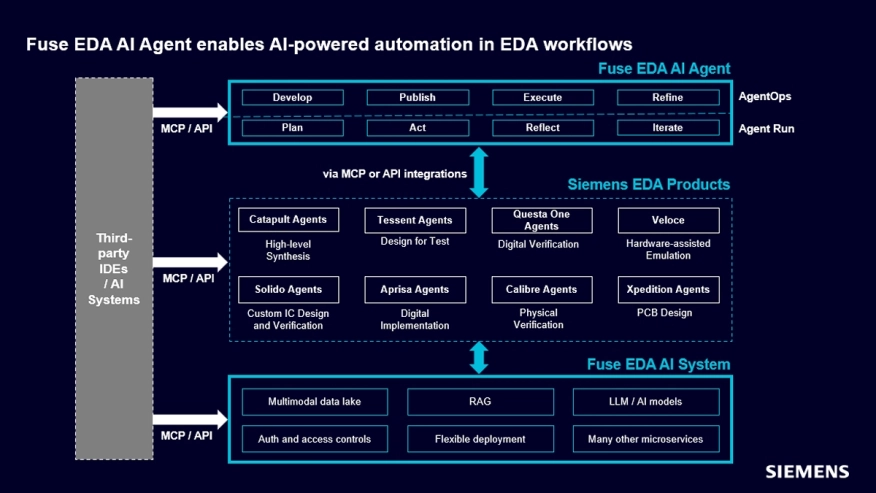 For faster engineers, generative EDA AI copilots were the industry’s first answer — but they are no longer sufficient. As design complexity and tool fragmentation accelerate, manual scripts and isolated point solutions fail to scale. Engineers need more than a chatbot; they need autonomous systems capable of intelligent reasoning, multi-step execution, and real-time adaptation across diverse EDA tools. This is the promise of agentic automation: a unified orchestration layer that delivers expert-level decision-making across the complete design lifecycle. Realizing it, however, requires overcoming domain-specific hurdles that generic AI frameworks are simply not equipped to handle.
To read the full article, click here
Related Semiconductor IP
- NPU IP
- JPEG XL Encoder
- I2C Master/Slave Controller Core
- NVMe Validation Test Suite
- Hybrid Memory Cube Verification IP
Related Blogs
- What is the EDA problem worth solving with AI?
- Teaching AI Agents to Speak Hardware
- Reimagining Chip Design - From Spec to Signoff with Cadence AI Super Agents
- Building Trusted AI Agents from the Silicon Root of Trust
Latest Blogs
- Tape-Out Readiness Checklist: Engineering Decisions That Prevent Costly Respins
- How Cadence DSPs Put In-Cabin AI Audio On-Chip in SemiDrive's X10
- The Fastest Path to Scalable Photonic Systems: Using Proven IP for both PIC and EIC designs
- Building Trusted AI Agents from the Silicon Root of Trust
- Heterogeneous Computing in Space