Vendor: Digital Blocks, Inc. Category: SPI Storage Controller

AMBA SPI Controller MRAM Controller

SPI Master Memory Controller IP core purpose-built for the Avalanche Technology AS30xG208 / ASAS308G208 family

Overview

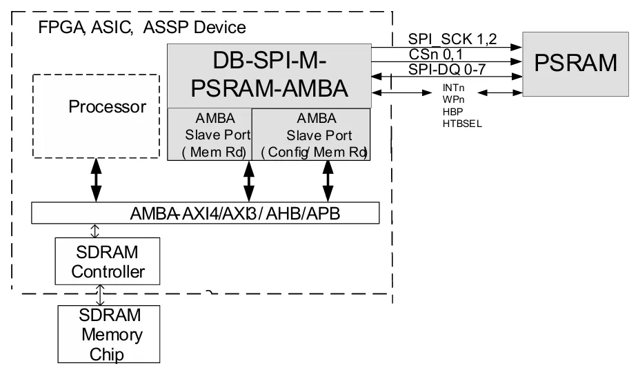
The DB-SPI-M-PSRAM-AXI4 is a SPI Master Memory Controller IP core purpose-built for the Avalanche Technology AS30xG208 / ASAS308G208 family of space-grade Dual Quad SPI Persistent SRAM (STT-MRAM) devices. It connects a host CPU subsystem to the P-SRAM through two AMBA slave interfaces: an AXI4-Lite port for control/status and FIFO-indirect command access, and an optional full AXI4 port that maps the P SRAM directly into the system address space for execute-in-place (XIP) code fetch and memory-mapped read/write data access. A configuration option available that excludes the XIP AXI4 interface, just for CPU access via shared config/data AXI4-Lite port.

The controller drives the dual-quad device in x8 lock-step (both quad dice in parallel, command/address mirrored, data byte-interleaved), as well as single-die x4 and x1 lane configurations, in both SDR and DDR (double transfer rate) timing. Because the P SRAM offers true SRAM write timing - no erase, no page programming, no program/erase status polling - the controller supports fully streaming memory-mapped writes as well as reads.

DB-SPI-M-PSRAM-AXI4 is a derivative of the production-proven Digital Blocks DB SPI Master controller family, retaining its clock-domain-crossing fabric, FIFO architecture, and AMBA interface blocks, with a datapath and engine set tailored to the Avalanche P-SRAM. It deliberately omits xSPI/JESD251 octal PHY and HyperRAM complexity, minimizing gate count and integration effort for designs standardizing on the AS30xG208.

Key features

  • Avalanche Technology AS30xG208 / ASAS308G208 space-grade Dual-Quad SPI P-SRAM (1 Gb - 8 Gb, STT-MRAM), including dual-die packages with independent CS1#/CLK1/IO[3:0] and CS2#/CLK2/IO[7:4] groups
  • Full instruction set: reads 03h/13h/0Bh/0Ch/0Dh/6Bh/6Ch/EBh/EDh, writes 02h/DAh/DEh/D2h/D1h, register access RDSR/RDFSR/WRSR/RDAR/WRAR, RDID, WREN/WRDI, QPI entry/exit (38h/FFh)
  • Device read-latency (MLATS) 0-15 cycles mapped one-to-one to the controller dummy-cycle engine (DCC)
  • XIP mode byte (Axh/Fxh) command-skip protocol for address-only streaming transactions, on reads and writes
  • WREN policy support: Normal, SRAM (WREN-less array writes), and Back-to-Back modes

Lane Configurations and Timing

  • x8 dual-quad lock-step: command/address broadcast to both dice, data byte-interleaved (even bytes die 1, odd bytes die 2); doubles read/write bandwidth
  • Single-die x4 (quad) and x1 (serial) operation, per-phase lane programming (1-1-1, 1-1-4, 1-4-4, 4-4-4 QPI)
  • SDR operation to 54 MHz SCK; DDR (DTR) operation to 40 MHz - up to 80 MB/s sustained in x8 DDR
  • SPI clock Mode 0 (CPOL=0/CPHA=0, SDR and DDR) and Mode 3 (CPOL=1/CPHA=1, SDR), matching the AS30xG208 exactly; illegal modes 1/2 are unreachable by hardware design

Host Interfaces

  • AXI4-Lite slave: control/status registers, TX/RX FIFO indirect command path, interrupt status/mask/vector registers
  • Optional AXI4 slave (compile-time XIP_PORT_EN): full memory-mapped read AND write access, INCR bursts to 256 beats, transparent chunking to SPI transactions, streaming read data path
  • Single interrupt output with 16-bit ISR/IMR/IVR bank; device INT1#/INT2# (per-die ECC/event) pins synchronized and surfaced as maskable interrupt sources

Block Diagram

Applications

  • Space and radiation-tolerant systems: boot/configuration memory, instrument data buffering, XIP code store on STT-MRAM
  • High-reliability industrial, avionics and defense systems requiring persistent low-latency memory without flash erase/wear management
  • Unified code + working-data memory: SRAM-timing writes allow the same device to serve as both non-volatile store and read/write data memory

What’s Included?

  • SystemVerilog RTL source (technology independent), parameterized single top level, synthesis filelist
  • Verification environment: testbench, AS30xG208 behavioral die model, 22 directed testcases, one command regression scripts (QuestaSim), functional coverage reporting
  • Reference synthesis timing constraints (SDC)
  • Bare-metal C driver with user guide (register definitions, init/read/write/mode APIs, reference application)
  • Linux platform driver (ioctl + memory-mapped port mmap), UAPI header, device-tree binding, test utility, user guide
  • Documentation: Technical Reference Manual + Rel 1.0.0 addendum, Integration Guide, simulation and testcase readmes

Specifications

Identity

Part Number
DB-SPI-M-PSRAM-AMBA
Vendor
Digital Blocks, Inc.
Type
Silicon IP

Files

Note: some files may require an NDA depending on provider policy.

Provider

Learn more about SPI Storage Controller IP core

Virtual Prototyping Platform with Flash Memory

In this paper we will see how the flash memories developed using Carbon Model Studio helps to bring up an ARM® Cortex A7 flash memory sub-system with primary and secondary boot codes. Flash memories system demonstrated here can be used for early boot code and driver development for any CPU based SoC.

Vertically Integrated MIPI Solutions

The emerging MIPI standards are designed to ensure interoperability among devices and software that are used in products for the exploding hand-held market. The standards facilitate the interconnection of multiple, mixed-signal integrated circuit devices on a single hand-held product. Use of the standards ensures low power, low pin count and interoperability of all the devices in the system and easy integration.

SoC Verification Flow and Methodologies

In this article, let me walk you through various verification methodologies we use for verifying IPs, Sub-systems, and SoCs and explain why we need new methodologies/standards like PSS.

Frequently asked questions about SPI Storage Controller IP cores

What is AMBA SPI Controller MRAM Controller?

AMBA SPI Controller MRAM Controller is a SPI Storage Controller IP core from Digital Blocks, Inc. listed on Semi IP Hub.

How should engineers evaluate this SPI Storage Controller?

Engineers should review the overview, key features, supported foundries and nodes, maturity, deliverables, and provider information before shortlisting this SPI Storage Controller IP.

Can this semiconductor IP be compared with similar products?

Yes. Buyers can compare this product with similar semiconductor IP cores or IP families based on category, provider, process options, and structured technical specifications.

×
Semiconductor IP