
Vendor: Macnica Category: V-By-One

V-by-One® HS plus Tx/Rx IP

High-speed serial interface compliant with V-by-One® HS plus standard IP core for FPGAs that supports “V-by-One® HS plus Standard…

Overview

High-speed serial interface compliant with V-by-One® HS plus standard

IP core for FPGAs that supports “V-by-One® HS plus Standard”, the next-generation high-speed interface standard technology developed by THine Electronics Inc.

V-by-One® HS plus Tx/Rx IP is an IP to enable Altera® FPGAs to send and receive signals compatible with the latest “V-by-One® HS plus Standard”.

Overview of V-by-One® HS plus Standard

V-by-One® HS plus is a next-generation high-speed interface standard proposed and developed by THine Electronics, Inc.. Key points are as follows:

  • Maximum transmission speed of 8Gbps/lane
    • Twice the speed of conventional technologies, supporting higher resolutions for LCD TVs, OLED TVs, etc., and higher refresh rates for gaming applications.
  • Cable reduction and slimming
    • Contributes to reduction in system cost and power consumption through cable reduction and slimming of transmission paths inside equipment.
  • Ensuring backward compatibility
    • Two modes are defined: "HS Mode," which has backward compatibility with conventional V-by-One® HS, and "HS plus Mode", which enables transmission at up to 8Gbps/lane.
  • Improved user convenience
    • Following the basic protocol and design concept of the existing V-by-One® HS, this next-generation high-speed interface standard has low hurdles for introduction.

IP Release Schedule (by Supported FPGA)

Altera® Devices

  • Arria® 10 GX FPGA
  • Cyclone® 10 GX FPGA
  • Agilex™ 7 FPGA           *Supported on F-Tile products.
  • Agilex™ 5 FPGA           *Please contact us.

Key features

Supported Configurations

  • Byte Mode
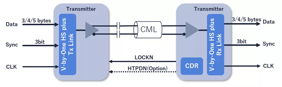
    • Supports 3-byte, 4-byte, or 5-byte modes.
  • Number of Lanes
    • Supports aggregation of up to 32 lanes.
  • Backward Compatibility
    • Supports both "HS Mode" and "HS plus Mode".

Transfer Speed

  • Maximum 8.0 Gbps/lane

Other Functions

  • Test Pattern Modes
    • Supports PRBS7, PRBS9, K28.1, and V-by-One HS plus
  • Inter-lane Deskew (at Rx)
    • Maximum 15 symbol clocks

Block Diagram

What’s Included?

  • Encrypted RTL (Verilog HDL)
  • Reference design
  • Simulation environment (For ModelSim)
  • User's manual
  • Reference design user's guide

Specifications

Identity

Part Number
V-by-One® HS plus Tx/Rx IP
Vendor
Macnica
Type
Silicon IP

Files

Note: some files may require an NDA depending on provider policy.

Provider

HQ: USA

Learn more about V-By-One IP core

The Benefits of a Multi-Protocol PMA

At Silicon Creations, we have developed a power and area optimized, flexible and programmable PMA (Physical Medium Attachment) architecture that can be reliably ported to different process nodes and scaled across protocol generations as data rates increase. It is called the Multi-Protocol PMA, or MP-PMA for short.

Frequently asked questions about V-by-One IP cores

What is V-by-One® HS plus Tx/Rx IP?

V-by-One® HS plus Tx/Rx IP is a V-By-One IP core from Macnica listed on Semi IP Hub.

How should engineers evaluate this V-By-One?

Engineers should review the overview, key features, supported foundries and nodes, maturity, deliverables, and provider information before shortlisting this V-By-One IP.

Can this semiconductor IP be compared with similar products?

Yes. Buyers can compare this product with similar semiconductor IP cores or IP families based on category, provider, process options, and structured technical specifications.

×
Semiconductor IP