Vendor: Arasan Chip Systems Inc. Category: Single-Protocol PHY

USB 2.0 PHY IP core

The USB 2.0 PHY IP core is a transceiver compliant with the USB 2.0 Transceiver Macrocell Interface Plus (UTMI+) level 3 specific…

Overview

The USB 2.0 PHY IP core is a transceiver compliant with the USB 2.0 Transceiver Macrocell Interface Plus (UTMI+) level 3 specification, for use with host, embedded host, On-the-Go (OTG) and function controllers. Its high speed, mixed-signal circuitry supports 480 Mb/s USB 2.0 High Speed (HS) traffic, while remaining backward compatible with USB 1.1 legacy protocol for 12Mb/s Full Speed (FS) traffic and 1.5Mb/s Low Speed (LS) traffic.

Arasan’s USB 2.0 PHY IP is also offered as a crystal-less PHY saving on the BoM.

The USB 2.0 PHY IP core performs low-level protocol and signaling functions. While transmitting, the PHY serializes data, generates Synchronize (SYNC) and End-of-Packet (EOP) packet fields, and performs bit stuffing and Non-Return-to-Zero Inverted (NRZI) encoding. While receiving data, the PHY recovers incoming data and clock, de-serializes data, strips SYNC and EOP fields, and performs bit un-stuffing and NRZI decoding.

FULL-FEATURED USB 2.0 PHY

The USB 2.0 PHY IP is a full-featured on-chip physical transceiver. It has Electro Static Discharge (ESD) protection and fully supports all OTG and host functionality. An optional charge pump generates a 5V supply to power external USB peripherals while in host mode. On-board clock generation and PLL blocks provide for accurate, high-speed data transmission from and to the transceiver. When this USB PHY core is used, a minimal number of external components is required.

Arasan is the among the industry’s first providers of USB IP with the launch of its USB 1.1 Device IP in 1996 and the industries ONLY provider to offer a Total USB 2.0 IP Solution which includes its USB 2.0 Host IP Core, USB 2.0 Device IP Core, USB 2.0 Hub IP, USB 2.0 OTG IP, the USB 2.0 PHY IP and software for multiple OS.
Key features

  • Complies with USB specifications, rev. 2.0 and 1.1
  • Complies with UTMI+ specification, level 3, rev. 1.0
  • Supports 480Mb/s (HS), 12Mb/s (FS) and 1.5MB/s (LS) serial data transmission rates
  • Supports 8-bit unidirectional Parallel Interface Engine (PIE) bus for HS, FS and LS modes, and Serial Interface Engine (SIE) for FS and LS modes
  • Supports USB 2.0-defined test modes
  • Supports OTG USB 2.0
  • Supports single-ended data interface
  • Digital I/O for Tx and Rx USB OTG cable status
  • Rail-to-rail common mode differential receiver
  • NRZI encoding and decoding
  • SYNC and EOP generation and detection
  • Bit stuffing and un-stuffing with error detection
  • Optional Charge Pump
  • Short-circuit protection for Charge Pump
  • Supports full junction temperature range of -40°C to 125°C
  • Dual 3.3V/1.2V supply
  • Integrated HS and FS/LS terminations
  • Area <1mm2 at 130nm
  • On-chip decoupling capacitors to minimize digital switching noise
  • Also offered as crystal-less PHY

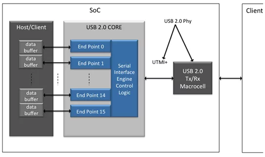
Block Diagram

Benefits

  • Silicon proven

What’s Included?

  • GDSII layout and layer map
  • Place-and-route views (.lib, .lef)
  • LVS and DRC verification reports
  • Verilog Sim Model (NC-Verilog)
  • Gate-level netlist and SDF timing
  • Test guidelines, layout guidelines and application notes

Specifications

Identity

Part Number
USB 2.0 PHY IP core
Vendor
Arasan Chip Systems Inc.
Type
Silicon IP

Standards & Interfaces

Supported Standards
USB 2.0

Files

Note: some files may require an NDA depending on provider policy.

Provider

Learn more about Single-Protocol PHY IP core

UFS Goes Mainstream

UniversalFlash Storage (UFS) was created for mobile applications and computer systems requiring high performance and low power consumption. These systems typically use embedded Flash based on the JEDEC standard eMMC. UFS was defined by JEDEC as the evolutionary replacement for eMMC offering significantly higher memory bandwidth. The standard builds on existing standards such as the SCSI command set, the MIPI Alliance M-PHY and UniPro as well as eMMC form factors to simplify adoption and development.

Universal Flash Storage: Mobilize Your Data

Universal Flash Storage (UFS) was created for mobile applications and computer systems requiring high performance and low power consumption. These systems typically use embedded Flash based on the JEDEC standard eMMC. UFS was defined by JEDEC as the evolutionary replacement for eMMC offering significantly higher memory bandwidth. The standard builds on existing standards such as the SCSI command set, the MIPI Alliance M-PHY and UniProSM as well as eMMC form factors to simplify adoption and development.

Arasan’s xSPI/eMMC5.1 PHY: Unified Dual-Mode Physical Layer IP

As SoCs evolve to support a growing range of memory interfaces, designers are faced with the challenge of balancing integration complexity, pin efficiency, and performance scalability. Traditionally, implementing both xSPI (JESD251) for boot and eMMC 5.1 for high-speed storage required separate PHYs, leading to increased silicon area, power consumption, and I/O overhead.

Frequently asked questions about Single-Protocol PHY IP

What is USB 2.0 PHY IP core?

USB 2.0 PHY IP core is a Single-Protocol PHY IP core from Arasan Chip Systems Inc. listed on Semi IP Hub.

How should engineers evaluate this Single-Protocol PHY?

Engineers should review the overview, key features, supported foundries and nodes, maturity, deliverables, and provider information before shortlisting this Single-Protocol PHY IP.

Can this semiconductor IP be compared with similar products?

Yes. Buyers can compare this product with similar semiconductor IP cores or IP families based on category, provider, process options, and structured technical specifications.

×
Semiconductor IP