Vendor: Arasan Chip Systems Inc. Category: Single-Protocol PHY

UHS-II PHY Core IP

The rapid proliferation of high-performance mobile and handheld devices has resulted in increasing requirements for non-volatile …

Overview

The rapid proliferation of high-performance mobile and handheld devices has resulted in increasing requirements for non-volatile memory. Memory interfaces with larger capacities and faster access times are needed.

In response to these trends, SD 4.1 UHS-II or sd 4.1 uhs-ii achieves a peak interface speed of 3.12Gb/s. Arasan’s UHS-II PHY is compliant with the draft specification of UHS-II and is an extremely area and power-efficient implementation. This interface is backward compatible with legacy SD cards. Both Host and Device UHS-II PHY configurations are available

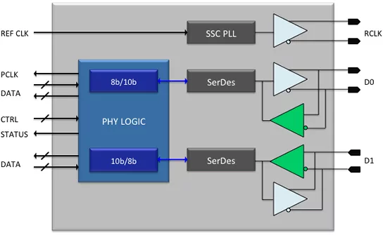
The UHS-II PHY IP is a comprehensive, silicon-proven configurable core that has been ported to multiple process nodes and leading foundries. It uses sub-LVDS signaling consisting of one pair each for transmit, receive, and an additional reference clock. This low-pin interface has reduced power consumption and low EMI. To further reduce power, the reference clock operates at 1/15 or 1/30 of the data transfer speed. This differential clock operates between 26MHz to 52MHz and is carried over the legacy SD lines DAT0, DAT1.

The SD 4.1 UHS-II PHY operates in both the Full-duplex and Half-duplex modes. It includes a 8b/10b encoder/decoder. The controller side interface of the UHS-II PHY operates in the range from 39MB/s to 156MB/s. The default data lane D0 is used for downstream connection and the D1 lane is used for the other direction. An 8b/10b coding scheme is used. To improve testability, the SD 4.1 UHS-II PHY implements the standard loopback paths.
Key features

  • Compliant to SD Specifications Part 1 UHS-II Specification Volume 2: PHY* and SD Specifications Part 1 UHS II Specification Volume 1: System and Protocol”
  • Per lane data rate between 390Mb/s to 1.56Gb/s
  • Supports peak interface speed of 3.12Gb/s (Half-duplex); 1.56Gb/s in Full-duplex mode
  • Sub-LVDS Differential PHY signaling
  • Low frequency differential reference clock (1/15 or 1/30) of data rate
  • Supports Spread Spectrum clocking to reduce EMI
  • Flexible transmission rates from 390Mb/s – 1.56Gb/s (each lane)
  • Multiple power saving modes: Dormant, Line standby
  • Low power, reduced EMI operationv
  • Integrated solution with built-in termination, no external components required
  • Easily ported to various process nodes and foundries

Block Diagram

Benefits

  • Silicon proven, fully compliant core
  • Premier direct support from Arasan IP core designers
  • Easy-to-use industry standard test environment
  • Unencrypted source code allows easy implementation
  • Reuse Methodology Manual guidelines (RMM) compliant verilog code

What’s Included?

  • GDSII database
  • LVS Netlist
  • Physical Abstract Model (LEF)
  • Timing Models
  • Behavioral Models
  • Design Integration Guide
  • Technical Documentation

Specifications

Identity

Part Number
UHS-II PHY Core IP
Vendor
Arasan Chip Systems Inc.
Type
Silicon IP

Files

Note: some files may require an NDA depending on provider policy.

Provider

Learn more about Single-Protocol PHY IP core

UFS Goes Mainstream

UniversalFlash Storage (UFS) was created for mobile applications and computer systems requiring high performance and low power consumption. These systems typically use embedded Flash based on the JEDEC standard eMMC. UFS was defined by JEDEC as the evolutionary replacement for eMMC offering significantly higher memory bandwidth. The standard builds on existing standards such as the SCSI command set, the MIPI Alliance M-PHY and UniPro as well as eMMC form factors to simplify adoption and development.

Universal Flash Storage: Mobilize Your Data

Universal Flash Storage (UFS) was created for mobile applications and computer systems requiring high performance and low power consumption. These systems typically use embedded Flash based on the JEDEC standard eMMC. UFS was defined by JEDEC as the evolutionary replacement for eMMC offering significantly higher memory bandwidth. The standard builds on existing standards such as the SCSI command set, the MIPI Alliance M-PHY and UniProSM as well as eMMC form factors to simplify adoption and development.

Arasan’s xSPI/eMMC5.1 PHY: Unified Dual-Mode Physical Layer IP

As SoCs evolve to support a growing range of memory interfaces, designers are faced with the challenge of balancing integration complexity, pin efficiency, and performance scalability. Traditionally, implementing both xSPI (JESD251) for boot and eMMC 5.1 for high-speed storage required separate PHYs, leading to increased silicon area, power consumption, and I/O overhead.

Frequently asked questions about Single-Protocol PHY IP

What is UHS-II PHY Core IP?

UHS-II PHY Core IP is a Single-Protocol PHY IP core from Arasan Chip Systems Inc. listed on Semi IP Hub.

How should engineers evaluate this Single-Protocol PHY?

Engineers should review the overview, key features, supported foundries and nodes, maturity, deliverables, and provider information before shortlisting this Single-Protocol PHY IP.

Can this semiconductor IP be compared with similar products?

Yes. Buyers can compare this product with similar semiconductor IP cores or IP families based on category, provider, process options, and structured technical specifications.

×
Semiconductor IP