Vendor: Macnica Category: SLVS-EC

SLVS-EC v3.0 Receiver IP

Next-generation CMOS image sensor interface, SLVS-EC v3.0, is implemented in FPGAs SLVS-EC v3.0 Rx IP is an interface IP core tha…

Overview

Next-generation CMOS image sensor interface, SLVS-EC v3.0, is implemented in FPGAs

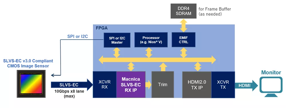
SLVS-EC v3.0 Rx IP is an interface IP core that runs on Altera® FPGAs. Using this IP, you can quickly and easily implement products that support the latest SLVS-EC standard v3.0. You will also receive an "Evaluation kit" for early adoption.

  • Altera® FPGAs can receive signals directly from the SLVS-EC Interface.
  • Compatible with the latest SLVS-EC Specification Version 3.0.
  • Supports powerful De-Skew function. Enables board design without considering Skew that occurs between lanes.
  • "Evaluation kit”(see below) is available for speedy evaluation at the actual device level.

Overview of SLVS-EC Standard

  • SLVS-EC (Scalable Low Voltage Signaling with Embedded Clock) is an interface standard for high-speed & high-resolution image sensors developed by Sony Semiconductor Solutions Corporation.
  • The SLVS-EC standard is standardized by JIIA (Japan Industrial Imaging Association).

Key features

  • SLVS-EC Specification Version 1.2/2.0 and the latest 3.0 are supported.
  • Provides various functions defined in the SLVS-EC Link Layer.
    • Selectable 32 or 64 pixel for output interface
    • Supports 8, 10, 12, 14, 16 bit/pixel
  • Realizes transfer with less overhead compared to conventional ANSI 8b10b by taking advantage of GCC (Gigabit Channel Coding) features added in the latest SLVS-EC Version 3.0.
  • Supports error correction using Error Correction Code (ECC)
  • Supports Byte to Pixel conversion in 1, 2, 4, 6, and 8 lane configurations.
  • Header analysis and payload error detection.
  • Compile options allow removal of unnecessary functions.

Block Diagram

Specifications

Identity

Part Number
SLVS-EC v3.0 Rx IP
Vendor
Macnica
Type
Silicon IP

Files

Note: some files may require an NDA depending on provider policy.

Provider

HQ: USA

Learn more about SLVS-EC IP core

The Benefits of a Multi-Protocol PMA

At Silicon Creations, we have developed a power and area optimized, flexible and programmable PMA (Physical Medium Attachment) architecture that can be reliably ported to different process nodes and scaled across protocol generations as data rates increase. It is called the Multi-Protocol PMA, or MP-PMA for short.

How silicon and circuit optimizations help FPGAs offer lower size, power and cost in video bridging applications

FPGAs are at home in the world of multi-gigabit-per-second signal conversion and bridging. In high-bandwidth telecoms, network and data center equipment, the FPGA is a mainstay of system designs, offering a valuable combination of high-speed SerDes capability, extensive logic resources, and programmability, giving designers the flexibility to modify features and functions without changing their board layout.

Frequently asked questions about SLVS-EC IP cores

What is SLVS-EC v3.0 Receiver IP?

SLVS-EC v3.0 Receiver IP is a SLVS-EC IP core from Macnica listed on Semi IP Hub.

How should engineers evaluate this SLVS-EC?

Engineers should review the overview, key features, supported foundries and nodes, maturity, deliverables, and provider information before shortlisting this SLVS-EC IP.

Can this semiconductor IP be compared with similar products?

Yes. Buyers can compare this product with similar semiconductor IP cores or IP families based on category, provider, process options, and structured technical specifications.

×
Semiconductor IP