Simulation VIP for Toggle NAND
In production since 2011 for many production designs.
Overview
In production since 2011 for many production designs.
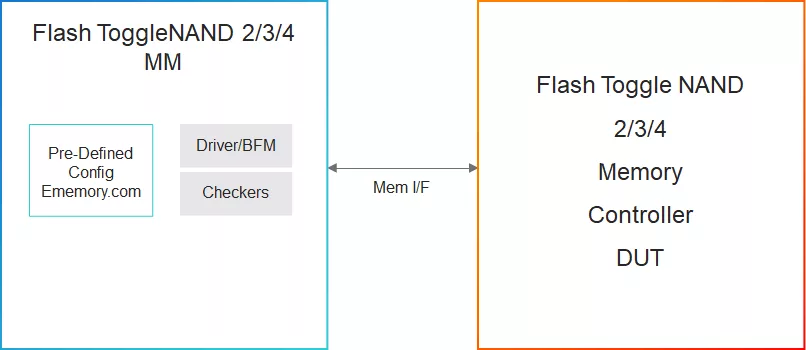
Cadence® Verification IP (VIP) for Toggle NAND is applicable to intellectual property (IP), system-on-chip (SoC), and system-level verification to provide verification of Flash NAND devices using toggle mode DDR 2.0 and above. The VIP for Toggle NAND is compatible with the industry-standard Universal Verification Methodology (UVM), runs on all leading simulators, and leverages the industry-standard Cadence Memory Model core architecture, interface, and use model.
Supported specification: toggle NAND DDR 2.0 Single-Level-Cell (SLC) and Multi-Level-Cell (MLC) devices as well as Toggle NAND DDR 3.0/4.0 Single-Level-Cell (SLC), Multi-Level-Cell, and Triple-Level-Cell (TLC) devices from Hynix, Samsung, Toshiba, and SanDisk.
Key features
- Speed
- Up to 200MHz or 400Mbps per DQ pin
- Up to 600MHz or 1200Mbps per DQ pin (Version 3.0/4.0)
- Bits per Cell
- Single-Level-Cell (SLC – 1-bit per cell) and Multi-Level-Cell (MLC – 2-bits per cell) devices support
- SLC, MLC and Triple-Level-Cell (TLC – 3-bits per cell) devices support (Version 3.0/4.0)
- Memory Sizes
- 64Gb, 128Gb, 256Gb, and 512Gb
- Configurability
- Page size in number of bytes
- Number of pages per block
- Number of blocks per Plane/LUN (die/stack)
- Number of Planes/LUNs per target
- Number of targets per device
- Commands
- Software Reset
- Read ID
- Read Status
- Read LUN status
- ODT turn on and off
- Operations
- Multi-Plane and Interleaved operations for Read, Cache Read, Program, and Erase Operation
- Multi-LUN Operations for simultaneous Read, Program, and Erase operations
- Multiple Die
- Supports Multiple Die with shared Chip Select signal
- Signals
- Differential signals support for Data Strobe Signal and Read Enable Signal
- LUN Features
- Supports LUN Set and Get Features to set NAND device in certain modes
Block Diagram
Specifications
Identity
Files
Note: some files may require an NDA depending on provider policy.

Provider
Learn more about NOR Flash IP core
Fastest Octal SPI Flash Interface Available Now From Cadence
Optimizing flash memory selection for automotive & other uses
When Memory Shortages Change Architecture Decisions
How silicon and circuit optimizations help FPGAs offer lower size, power and cost in video bridging applications
Functional, Fast, and Ultra-Low Power: A Live Look at Weebit's Second IP Module
Frequently asked questions about NOR Flash Interface IP
What is Simulation VIP for Toggle NAND?
Simulation VIP for Toggle NAND is a NOR Flash IP core from Cadence Design Systems, Inc. listed on Semi IP Hub.
How should engineers evaluate this NOR Flash?
Engineers should review the overview, key features, supported foundries and nodes, maturity, deliverables, and provider information before shortlisting this NOR Flash IP.
Can this semiconductor IP be compared with similar products?
Yes. Buyers can compare this product with similar semiconductor IP cores or IP families based on category, provider, process options, and structured technical specifications.