Vendor: Cadence Design Systems, Inc. Category: NOR Flash

Simulation VIP for ONFi

Gold standard for JEDEC® ONFI memory device for your IP, SoC, and system-level design verification.

Verification IP Controller View all specifications

Overview

Gold standard for JEDEC® ONFI memory device for your IP, SoC, and system-level design verification.

In production since 2011 for dozens of production designs.

The Cadence® Memory Model Verification IP (VIP) for ONFi is the verification solution for NAND flash memory interface based on any version of the Open NAND Flash interface. The VIP supports all the interfaces: SDR, NV-DDR, NV-DDR2, NV-DDR3, and NV-LPDDR4, as defined in the standard. The interface mode can be dynamically switched from one to another during the simulation till NV-DDR2. Through the "Volume Address" feature, defined in the latest standard, any number of device models can be connected to a single "chip enable" signal to allow testing of CE_n pin reduction scenarios.

Supported specification: JEDEC ONFi versions 1.0, 2.0, 3.0, 4.0, 4.1, 4.2, 5.0, 5.1, and 5.2

Key Features

The following table describes key features from the specifications that are implemented in the VIP:

Feature Name

Description

Speed

  • NV-DDR: 200 MT/s (DDR)
  • NV-DDR2: 800 MT/s (DDR)
  • NV-DDR3: 3600MT/s (DDR)
  • NV-LPDDR4: 4800MT/s (DDR)

Interfaces

  • SDR, NV-DDR, NV-DDR2, NV-DDR3, and NV-LPDDR4. Ability to switch among interface modes dynamically. Available on low-voltage operation of the device to provide faster throughput and improved I/O Power consumption

General Functionality

  • Reset, read device ID parameters, read status of NAND device and LUNs, multi-plane read, cache read, program, erase, and copyback operations, multi-LUN operations, LUN get/set commands, ZQ calibration, set/get feature addresses.

Core and Bus timing

  • Setup/hold, per lane or per bit, pulse width

Timing Modes

  • Timing modes up to timing mode 26

Training

  • Explicit and implicit DCC training, read DQ training, write DQ training at TX side

CE_n Pin Reduction

  • Allows multiple devices, model instances, to be connected to a single "chip enable"

Data Eye

  • User configurable timing parameters to corrupt data eye during read path

ONFI 5.0 Features

  • ODT disable and enable commands, DBI

ONFI 5.1 Features

  • Differential signaling on power up
  • Trainings: Per-pin VrefQ adjustment
  • Supported parameters page for new trainings and timing modes
  • New feature addresses for WDCA and per-pin VrefQ training

ONFI 5.2 Features

  • Separate Command Address (SCA) mode with NV-LPDDR4
  • CA packets decoding and execution
  • Command interleaving
  • Unmatched DQS
  • SCA timing checks
  • SCA initialization checks
  • CA training

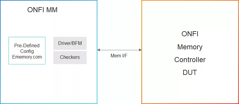
Block Diagram

Benefits

  • Hundreds of protocol and timing checkers to easily catch design bugs
  • Hundreds of predefined configurations based on specific memory vendors' part numbers, datasheets, or generic JEDEC definitions available on ememory.com(opens in a new tab)
  • Transaction and memory callbacks for all protocol, model states and device memory events
  • Error injection capability through user modification of transaction contents
  • Ability to check for errors and change error severity
  • Ability to dynamically change configuration parameters
  • Packet tracker creation for easy debugging
  • Support testbench language interfaces for SystemVerilog and UVM

Specifications

Identity

Part Number
Simulation VIP for ONFi
Vendor
Cadence Design Systems, Inc.
Type
Verification IP
Controller / PHY
Controller

Files

Note: some files may require an NDA depending on provider policy.

Provider

Learn more about NOR Flash IP core

Optimizing flash memory selection for automotive & other uses

Over the past few years, there has been an increasing demand for NOR Flash memory for use in automotive applications. Initial uses included applications such as infotainment and engine control. However, as advancements in automotive computerization continue to progress, NOR Flash memory is seeing use in a wider range of various automotive applications.

When Memory Shortages Change Architecture Decisions

For decades, the choice between embedded and external Non-Volatile Memory (NVM) in semiconductor designs has been straightforward. External memory, such as EEPROM, NOR Flash, or NAND Flash, offered lower cost per bit and greater flexibility, making a two-die architecture the default choice across a wide range of applications. That assumption is now being challenged.

How silicon and circuit optimizations help FPGAs offer lower size, power and cost in video bridging applications

FPGAs are at home in the world of multi-gigabit-per-second signal conversion and bridging. In high-bandwidth telecoms, network and data center equipment, the FPGA is a mainstay of system designs, offering a valuable combination of high-speed SerDes capability, extensive logic resources, and programmability, giving designers the flexibility to modify features and functions without changing their board layout.

Frequently asked questions about NOR Flash Interface IP

What is Simulation VIP for ONFi?

Simulation VIP for ONFi is a NOR Flash IP core from Cadence Design Systems, Inc. listed on Semi IP Hub.

How should engineers evaluate this NOR Flash?

Engineers should review the overview, key features, supported foundries and nodes, maturity, deliverables, and provider information before shortlisting this NOR Flash IP.

Can this semiconductor IP be compared with similar products?

Yes. Buyers can compare this product with similar semiconductor IP cores or IP families based on category, provider, process options, and structured technical specifications.

×
Semiconductor IP