Vendor: Arasan Chip Systems Inc. Category: Single-Protocol PHY

ONFI 5.0 NAND Fash PHY IP Compliant to JEDEC

Open NAND Flash Interface (ONFI) for NAND Flash Memory chips is an open standard.

Overview

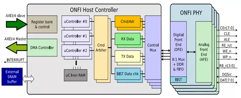
Open NAND Flash Interface (ONFI) for NAND Flash Memory chips is an open standard. The ONFI 5.0 PHY IP is designed to connect seamlessly with their ONFI 5.0 Host Controller IP. The ONFI 5.0 PHY has complete SDR, NV-DDR, NV-DDR2, NV-DDR3 and NV-LPDDR4 TX/RX functionality and supports all the speeds defined in the ONFI specification while remaining backwards compatible with the prior versions of the ONFI specifications.  The ONFI 5.0 PHY enables data training, various power drives and ZQ calibration, which ensures maximum operating speed and optimum signal integrity. The PHY uses a PLL / DLL combination to provide very flexible frequency access.  The PHY also includes ESD protection on all the various ONFI interface pins. The ONFI 5.0 PHY is an area efficient with a low power consumption and the IO library supports all the features mentioned in the ONFI 5.0 specifications.
Key features

  • Designed for seamless integration with Arasan’s ONFI 5.0 Host Controller IP.
  • The PHY design supports the newly introduced NV-LPDDR4 mode along with SDR, NV_DDR, and NV_DDR2, NV_DDR3 mode.
  • Supports IO voltages at 1.2 V and 1.8 V with core voltage at 0.8V +/-10% and auxiliary power supply at 1.8V +/-10%.
  • Includes ONFI 5.0 data I/O PADS and auxiliary I/O PADS with ESD protection structures.
  • Includes on-die termination and differential signaling for improved signal integrity at high speeds.
  • Integrate PLL and Clock divider to support ONFI 5.0 different mode frequencies.
  • Integrate a Master Slave DLL for tuning the Receive clock DQS modes.
  • The clock generator {PLL, DLL & CLKDIVIDER} is designed to support different modes of ONFI 4.2 frequencies {20MHz to 860MHz}.
  • Built-in diagnostics for monitoring the PLL, DLL and clock divider.
  • Includes fractional delay logic in Digital front end of the PHY to correct for skew on both input and output.
  • In the Analog Front End (AFE) PHY, CALIO PAD automatically calibrates the source and sink impedance of ONFI I/O and the ODT (On Die Termination) resistors.

Block Diagram

Specifications

Identity

Part Number
ONFI 5.0 NAND FLASH PHY IP Compliant to JEDEC
Vendor
Arasan Chip Systems Inc.
Type
Silicon IP

Files

Note: some files may require an NDA depending on provider policy.

Provider

Learn more about Single-Protocol PHY IP core

UFS Goes Mainstream

UniversalFlash Storage (UFS) was created for mobile applications and computer systems requiring high performance and low power consumption. These systems typically use embedded Flash based on the JEDEC standard eMMC. UFS was defined by JEDEC as the evolutionary replacement for eMMC offering significantly higher memory bandwidth. The standard builds on existing standards such as the SCSI command set, the MIPI Alliance M-PHY and UniPro as well as eMMC form factors to simplify adoption and development.

Universal Flash Storage: Mobilize Your Data

Universal Flash Storage (UFS) was created for mobile applications and computer systems requiring high performance and low power consumption. These systems typically use embedded Flash based on the JEDEC standard eMMC. UFS was defined by JEDEC as the evolutionary replacement for eMMC offering significantly higher memory bandwidth. The standard builds on existing standards such as the SCSI command set, the MIPI Alliance M-PHY and UniProSM as well as eMMC form factors to simplify adoption and development.

Arasan’s xSPI/eMMC5.1 PHY: Unified Dual-Mode Physical Layer IP

As SoCs evolve to support a growing range of memory interfaces, designers are faced with the challenge of balancing integration complexity, pin efficiency, and performance scalability. Traditionally, implementing both xSPI (JESD251) for boot and eMMC 5.1 for high-speed storage required separate PHYs, leading to increased silicon area, power consumption, and I/O overhead.

Frequently asked questions about Single-Protocol PHY IP

What is ONFI 5.0 NAND Fash PHY IP Compliant to JEDEC?

ONFI 5.0 NAND Fash PHY IP Compliant to JEDEC is a Single-Protocol PHY IP core from Arasan Chip Systems Inc. listed on Semi IP Hub.

How should engineers evaluate this Single-Protocol PHY?

Engineers should review the overview, key features, supported foundries and nodes, maturity, deliverables, and provider information before shortlisting this Single-Protocol PHY IP.

Can this semiconductor IP be compared with similar products?

Yes. Buyers can compare this product with similar semiconductor IP cores or IP families based on category, provider, process options, and structured technical specifications.

×
Semiconductor IP