Arasan to demonstrate the industry's first MIPI SWI3S™ IP at the MIPI Member meet in Taipei
Arasan provides a Total SWI3S™ IP Solution including the SWI3S™ PHY which will be available on multiple foundry nodes 22nm and below.
The Open NAND Flash Interface (ONFI) is an Open standard for NAND Flash Memory chips.
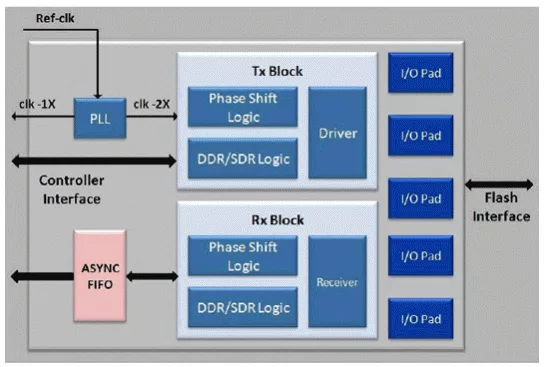
The Open NAND Flash Interface (ONFI) is an Open standard for NAND Flash Memory chips. ONFI seeks to standardize the low-level interface. ONFI 3.2 is the standard for a High-Speed NAND Flash interface. It has multiple modes of operation like SDR, NV-DDR and NV-DDR2 modes. Micron’s Clear NAND operations such as Queue page read and Program page pause, Program page resume, Program page delay are also supported. ONFI 3.2 PHY extends the benefits of ONFI 3.x and 2.3 standards. It provides a high-speed interface supporting transfer rates up to 400 MT/s. It also supports the EZ-NAND interface. Lots of performance-enhancing features like Interleaving operations, Multi-plane operations is supported. ONFI 3.2 PHY incorporates the full TX/RX logic for NV-DDR2/NV-DDR mode of operation and is backward compatible to the SDR mode of operation. ONFI 3.2 improves on version ONFI 3.0 with more robust power sequencing to protect NAND flash, more flexible timing to support NAND usage in different topologies, improved parameters for testing, and other enhancements. Included in the OFNI 3.2 PHY is a set of high-speed I/O pads compatible to ONFI 1.8v 266 MHz NV-DDR2 and 3v 100 MHz NV-DDR.
Note: some files may require an NDA depending on provider policy.

ONFI 3.2 NAND Flash PHY IP Compliant to JEDEC is a Single-Protocol PHY IP core from Arasan Chip Systems Inc. listed on Semi IP Hub.
Engineers should review the overview, key features, supported foundries and nodes, maturity, deliverables, and provider information before shortlisting this Single-Protocol PHY IP.
Yes. Buyers can compare this product with similar semiconductor IP cores or IP families based on category, provider, process options, and structured technical specifications.