Dual Channel 8b D/A Converter - TSMC T40ULP
A Dual Channel 8b D/A converter is provided with TSMC T40ULP+ESF3 wafer process. I
Overview
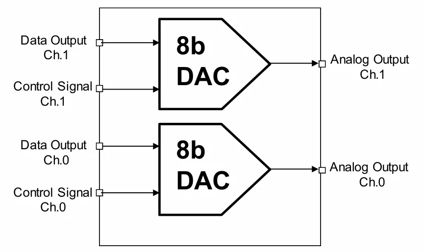
A Dual Channel 8b D/A converter is provided with TSMC T40ULP+ESF3 wafer process. It is voltage output D/A Converter, with supporting the wide supply range from 1.62 to 3.63V. It was employed the novel architecture. It enhances the linearity and reduces the current consumption.
Key features
- 8b resolution
- Dual Channel
- Ultra low Current consumption.
- 30µs conversion time with 1pF capacitive load
- Excellent Linearity
- suitable for the reference voltage generator for the comparators
Block Diagram
Silicon Options
| Foundry | Node | Process | Maturity |
|---|---|---|---|
| TSMC | 40nm | ULP | Available on request |
Specifications
Identity
Files
Note: some files may require an NDA depending on provider policy.
Provider
Learn more about DAC IP core
Making the most of the 60th DAC
DAC 2022 - Is it too risky not to adopt RISC-V?
Specifying a PLL Part 1: Calculating PLL Clock Spur Requirements from ADC or DAC SFDR
DAC: The View from Wall Street
DAC Panelists Discuss Emulation's Versatility & Various Use Models
Frequently asked questions about DAC IP cores
What is Dual Channel 8b D/A Converter - TSMC T40ULP?
Dual Channel 8b D/A Converter - TSMC T40ULP is a DAC IP core from Renesas listed on Semi IP Hub. It is listed with support for tsmc Available on request.
How should engineers evaluate this DAC?
Engineers should review the overview, key features, supported foundries and nodes, maturity, deliverables, and provider information before shortlisting this DAC IP.
Can this semiconductor IP be compared with similar products?
Yes. Buyers can compare this product with similar semiconductor IP cores or IP families based on category, provider, process options, and structured technical specifications.