Vendor:
Truechip Solutions
Category:
DDR
DDR5 Verification IP
The DDR5 Verification IP provides an effective & efficient way to verify the components interfacing with DDR5 interface of an ASI…
Overview
The DDR5 Verification IP provides an effective & efficient way to verify the components interfacing with DDR5 interface of an ASIC/FPGA or SoC. The DDR5 VIP is fully compliant with Standard DDR5 specification from JEDEC. This VIP is a light weight with an easy plug-and-play interface so that there is no hit on the design time and the simulation time.
Key features
- Compliant to JEDEC DDR5 SDRAM Specification.
- Supports connection to any DDR5 Memory Controller IP communicating with a JEDEC compliant DDR5 Memory Model.
- Supports configurable SDRAM addressing of different sizes (x4,x8 and x16).
- Available in all memory sizes from upto 64 Gb.
- Supports Data Bus Inversion(DBI).
- Supports Data Masking(DM).
- Supports Cyclic Redundancy Check (CRC)
- Support for all speed-grades/speed-bins.
- Supports Programmable burst lengths.
- Supports configurable timing parameters and rank associations.
- Supports capturing all the valid DDR5 commands including Activate, Read Write, Precharge.
- Supports CA parity for command/address bus.
- Supports Power-up Reset and initialization sequences.
- Supports Precharge Power-Down, Active Power-Down, Self-Refresh operation.
- Reports various timing errors, which can be used to check any timing violations.
- Provides full control to the user to enable / disable various types of messages.
- Supports full timing models or bus functional models.
- Support for Multiple Ranks architecture.
- Supports advanced SystemVerilog features like constrained random testing.
- Supports dynamically configurable modes.
- Strong Protocol Monitor with real time exhaustive programmable checks.
- Supports Dynamic as well as Static Error Injection scenarios.
- On the fly protocol checking using protocol check functions, static and dynamic assertion.
- Built in Coverage analysis.
- Provides a comprehensive user API (callbacks) in Monitor, Controller and Memory Model BFMs.
- Graphical analyser to show transactions for easy debugging.
Block Diagram
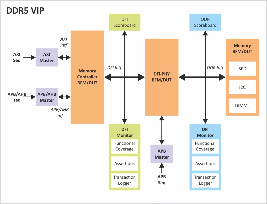
DDR5/4/3 block diagram
Benefits
- Available in native SystemVerilog (UVM/OVM/VMM) and Verilog
- Unique development methodology to ensure the highest levels of quality
- 24X5 customer support & response under 90 Min.
- Unique and customizable licensing models
- Exhaustive set of assertions and cover points with connectivity examples for all the components
- Consistency of interface, installation, operation and documentation across all our VIPs
- Provide complete solution and easy
What’s Included?
- DDR5-SDRAM Model
- DDR5 Monitor & Scoreboard
- DDR5 Memory Controller BFM/Agent
- DDR5 PHY BFM model
- DDR5 Phy Monitor and Scoreboard
- Test-Bench Configurations
- Test Suite (Available in Source code)
- Basic Protocol Tests
- Directed & Random Tests
- Assertions & Cover Point Tests
- Integration Guide, User Manual and Release Notes
Specifications
Identity
Part Number
DDR5/4/3
Vendor
Truechip Solutions
Type
Verification IP
Controller / PHY
Controller
Standards & Interfaces
Memory
DDR5
Files
Note: some files may require an NDA depending on provider policy.
Provider

HQ:
USA
Learn more about DDR IP core
Why eMMC is still a good low-budget storage option?
Revolutionizing Electronic Circuit Testing and Debugging Using JTAG
Is DisplayPort really the future standard?
Truechip Announces First Customer Shipment Of USB4v2 Verification IP
Truechip, today announced that it has shipped early adoption version of USB4v2 Verification IP.
Truechip: Exhibiting and Showcasing Latest Verification IPs and NOC IPs at Design Automation Conference (DAC) 2023
Truechip is exhibiting and showcasing its capabilities at the 60th Design Automation Conference (DAC) 2023, starting from July 9–13, 2023, at Moscone Center West in San Francisco, CA at booth # 2544, Level-II.
Frequently asked questions about DDR Interface IP
What is DDR5 Verification IP?
DDR5 Verification IP is a DDR IP core from Truechip Solutions listed on Semi IP Hub.
How should engineers evaluate this DDR?
Engineers should review the overview, key features, supported foundries and nodes, maturity, deliverables, and provider information before shortlisting this DDR IP.
Can this semiconductor IP be compared with similar products?
Yes. Buyers can compare this product with similar semiconductor IP cores or IP families based on category, provider, process options, and structured technical specifications.