Vendor: Cadence Design Systems, Inc. Category: DDR

Simulation VIP for DDR4

In production since 2011 on dozens of production designs.This Cadence® Verification IP (VIP) supports the JEDEC® Low Power Memory…

Verification IP Controller DDR4 View all specifications

Overview

In production since 2011 on dozens of production designs.

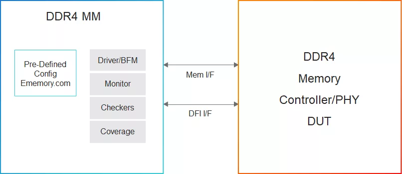
This Cadence® Verification IP (VIP) supports the JEDEC® Low Power Memory Device, DDR4 SDRAM standard. It provides a mature, highly capable compliance verification solution that supports simulation, and formal analysis, making it applicable to intellectual property (IP), system-on-chip (SoC), and system-level verification. The DDR4 SDRAM VIP is compatible with the industry-standard Universal Verification Methodology (UVM), runs on all leading simulators, and leverages the industry-standard Cadence Memory Model core architecture, interface, and use model.

DDR4 standard is the next generation of DRAM device memory standard with many improvements in performance, reliability and power saving over the previous generation of DRAM devices (DDR3). With data centers, cloud computing, and number of cores in a system increasing every day, there is a demand for high capacity and more bandwidth. With the increase in the capacity and bandwidth percentage of power consumed by memories, power consumed by the whole system is also increasing and price, performance, and watt is becoming more important as well. DDR4 addresses most of these issues with increased bandwidth, capacity, new power saving features, and with more reliability through CRC and Parity. DDR4 is not backwards compatible with DDR3.

Supported specification: JEDEC JESD79-4B specification and 3DS extensions.
Key features

  • Data Width, Density
    • 4, 8, and 16. 2 Gb to 16 Gb
  • Speed
    • 1600, 1866, 2133, 2400, 2666, and 3200
  • Bank Groups
    • Modeling the concept and the timing associated with the back-to-back accesses to the same and difference bank group
  • General DDR Functionality and Timing Checks
    • Precharge, Activate, Read, Write, Mode Register Write, Write leveling, ODT checks, Power Down, Self Refresh, Initialization, and all related timing checks
  • Reduced Pin Count
    • A16..A14 are multiplexed with ras, cas and webar pins and dedicated act pin for Activate command
  • Parity Error Injection
    • Supports Parity Error injection using callbacks
  • 3DS Level
    • Supports command decoding
  • 3DS Read and Write
    • Supports 3DS Read and Write commands for 2H, 4H, and 8H combinations
  • More Read Training Options
    • More MPR registers organized as pages. More options of reading those registers and preamble training
  • Reading of Mode Register Settings
    • Some important setting of the more registers are shadowed into page-2 MPRs
  • Data Mask and Data Bus Inversion
    • Data on the bus can be inverted during both read and write to save power. Both Data Mask and Data Bus inversion features can be set using mode registers
  • Per-DRAM Addressing
    • Allows mode registers of each DRAM on the DIMM to be programmed independently
  • CAL Mode
    • Allows CSBAR to be asserted a few cycles before actual command details
  • Write CRC
    • CRC is checked for writes and passes the error to the controller. CRC failures will let the write go through if Data Mask is disabled, and will block writes if that Mask is enabled
  • Parity
    • Parity checking is off by default, but when enabled parity is checked for each command before execution and also detailed recovery in case of errors and reporting of logs through MPR Reads
  • Control Gear Down Mode
    • Allows the DRAM to operate in 2N mode
  • Jitter, Drift, and Skews
    • Support of tDQSCK jitters, drift per operating voltage and temperature and skew
  • Configurable Preamble
    • Allows both 1CK and 2CK preambles to be selected for both read and write
  • Refresh Options
    • Normal mode refresh, self refresh, temperature controller self refresh, Low Power Array self refresh, and fine-granularity refresh
  • Maximum Power Saving Mode
    • Preserves the mode register settings, but loses data
  • RTT
    • Complete modelling of all RTT values, RTT_NOM, RTT_Park, and RTT_Wr with the internal register representing the value of RTT at a given point of time, based on the mode of operation
  • Connectivity Test Mode
    • Allows DRAM to enter CT Mode when Test Enable (TEN) pin is asserted HIGH

Block Diagram

Specifications

Identity

Part Number
Simulation VIP for DDR4
Vendor
Cadence Design Systems, Inc.
Type
Verification IP
Controller / PHY
Controller

Standards & Interfaces

Memory
DDR4

Files

Note: some files may require an NDA depending on provider policy.

Provider

Learn more about DDR IP core

DFI 6.0 Key Highlights of the Latest DFI Specification

DFI 6.0.1 (also referred to as DFI 6.0 in the rest of the blog) is the latest standard of the DFI specification. It removes support for earlier DDR/LPDDR generations, adds support for LPDDR6 and HBM4, adds/modifies low-power features, reorganizes WCK and memory-error handling, removes the disconnect protocol, and adds support for 1:3 and 1:6 DFI ratios.

SOCAMM: Modernizing Data Center Memory with LPDDR6/5X

Small Outline Compression-Attached Memory Module (SOCAMM) has made its way into the data center as an alternative to external CPU memory, due to its high performance, low power, memory capacity, and scalability.

Heterogeneous Multicore using Cadence IP

This blog presents a heterogeneous multicore system built with the RISC-V Host CPU and Cadence IP: Xtensa DSPs, and the Janus Network-on-Chip (NoC). While this example uses an RISC-V CPU, any other ISA with similar capabilities can also serve as the host CPU.

The Power of Shifting Left: Cadence Accelerating Innovation with Arm

In semiconductor design, projects are remembered for their extremes—legendary successes and cautionary failures. The difference often hinges on when problems are discovered. A bug found late in development can derail timelines and budgets. This is why "shifting left"—moving testing and validation earlier in the process—is now a critical strategy for innovation.

Boosting AI Performance with CXL

AI workloads are outpacing traditional memory architectures—but CXL®︎ offers a smarter path forward. Cadence's blog, "Boosting AI Performance with CXL," outlines how CXL enables dynamic memory expansion, memory sharing, and maintains coherency across devices to eliminate bottlenecks and boost performance for processing training and inference in large-scale AI systems.

Cadence Drives Next-Gen Memory and Connectivity at FMS 2025

Cadence continues to invest significant engineering effort to deliver advanced, user-friendly IP solutions across a range of essential protocols, two of which were on display at the recent Future of Memory and Storage (FMS) conference in Santa Clara, CA.

Frequently asked questions about DDR Interface IP

What is Simulation VIP for DDR4?

Simulation VIP for DDR4 is a DDR IP core from Cadence Design Systems, Inc. listed on Semi IP Hub.

How should engineers evaluate this DDR?

Engineers should review the overview, key features, supported foundries and nodes, maturity, deliverables, and provider information before shortlisting this DDR IP.

Can this semiconductor IP be compared with similar products?

Yes. Buyers can compare this product with similar semiconductor IP cores or IP families based on category, provider, process options, and structured technical specifications.

×
Semiconductor IP