Vendor: Cadence Design Systems, Inc. Category: DDR

Simulation VIP for DDR4 LRDIMM

First to market with full DDR4 LRDIMM support.This Cadence® Verification IP (VIP) supports the JEDEC® DDR4 Unbuffered DIMM (UDIMM…

Verification IP Controller DDR4 View all specifications

Overview

First to market with full DDR4 LRDIMM support.

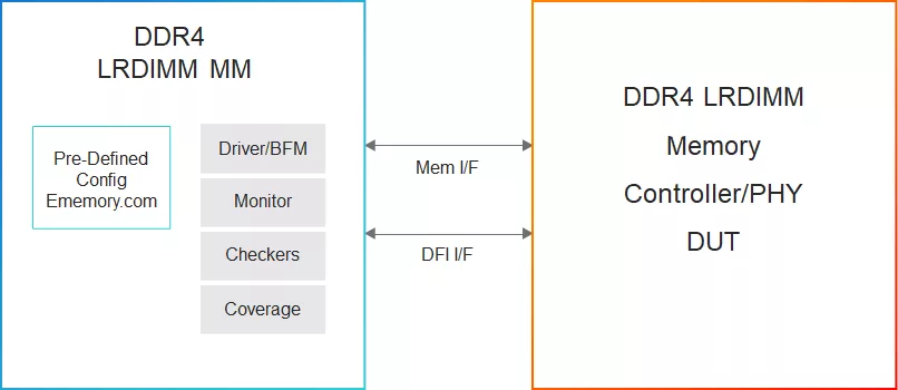
This Cadence® Verification IP (VIP) supports the JEDEC® DDR4 Unbuffered DIMM (UDIMM), Registered DIMM (RDIMM), and Load-Reduced DIMM (LRDIMM) design standards. It provides a mature, highly capable compliance verification solution that supports simulation and formal analysis, making it applicable to intellectual property (IP), system-on-chip (SoC), and system-level verification. The DDR4 RDIMM Memory Model VIP is compatible with the industry-standard Universal Verification Methodology (UVM), runs on all leading simulators, and leverages the industry-standard Cadence Memory Model core architecture, interface, and use model.

DDR4 DIMM is the next generation DIMM specification with improvements in the areas of speed, configuration, reliability, and power saving. It supports speeds up to 3200 speed grade. With redefined Control Word Write, DRAM Mode register write interface, and with new control word settings like programmable latency and encoded quad modes, it is more flexible. Guarding of the command forwarded to DRAMs and the RCD Control word writes with optional parity checking and detailed specification for different ways of recovery in the case of parity errors makes this more reliable.

Supported specification: DDR4 SDRAM UDIMM Design Specification Revision 1.00, DDR4 SDRAM RDIMM Design Specification Revision 1.00, DDR4 SDRAM Load-Reduced DIMM Design Specification Revision 1.00, DDR4RCD02 Revision 1.00, and DDR4DB02 Revision 1.00.
Key features

  • DIMM Types
    • DDR4 UDIMM, RDIMM, LRDIMM, DDR4 3DS, 3DS UDIMM, 3DS RDIMM, and 3DS LRDIMM
  • LRDIMM Training Modes
    • Fully supports DWL, HWL, MREP, MRD, and MWD Training modes
  • Initialization and Reset
    • Use Power Up Reset and Reset with Stable Power with all timing and pin validity checks
  • Weak Driver Support
    • Supports signal strength modeling. Users can use pull up or pull down on the input pins and the model detects the signal strength and function like a real device
  • New DIMM Configuration Support
    • Raw Cards with CB bits are mapped to the middle of DQ and DQS buses
  • Configurable DIMM Topology
    • A number of ranks and components with and the overall interconnect between DIMM, RCD, and DRAM are configurable using SOMAs
  • Flyby Delays
    • Supports Flyby delay to specify wiring delays for UDIMM, RDIMM and LRDIMM. Can be changed on the fly
  • ECC Checks Bits
    • Optional DRAM instantiation for checks bits
  • Address Mirroring
    • RDIMM will optionally mirror the address bits as mentioned in specification
  • DQ Maps
    • Configurable DQ Maps to match one of the options mentioned in the specification
  • Core RCD Forwarding Logic
    • DRAM MRS command handling, inversion, mirroring, command latency, propagation delay, gating with parity checks, and different CS modes
  • RCD Control Word Writes
    • MRS7 interface for CWW and most of the control word settings
  • Parity
    • Supports optionally checking for even parity. CWW and DRAM commands support gating errors
    • Implements different recovery mechanisms defined in the specification
  • CA Training
    • Supports Clk to CA and ODT, CKE, CSBAR loop-back modes
  • DB Control Word Writes
    • MRS7 interface for Buffer Control Word Writes and most of the control word settings
  • DB Data Latching and Forwarding
    • Latching of Read and Write data to forward it to Host, or the DRAM side depending on the command
  • DDR4 DB Delay Registers
    • Supports all the Nibble and bit-lane delay registers mentioned in the specification
  • DB Command Sequence and Parity
    • Supports the command sequence and Parity error along with the relevant buffer Control Words
  • LRDIMM Rank to Rank Timing Checks
    • Supports timing check for Read and Write accesses to different Ranks
  • DRAM Features
    • Supports all DDR4 SDRAM features

Block Diagram

Specifications

Identity

Part Number
Simulation VIP for DDR4 LRDIMM
Vendor
Cadence Design Systems, Inc.
Type
Verification IP
Controller / PHY
Controller

Standards & Interfaces

Memory
DDR4

Files

Note: some files may require an NDA depending on provider policy.

Provider

Learn more about DDR IP core

DFI 6.0 Key Highlights of the Latest DFI Specification

DFI 6.0.1 (also referred to as DFI 6.0 in the rest of the blog) is the latest standard of the DFI specification. It removes support for earlier DDR/LPDDR generations, adds support for LPDDR6 and HBM4, adds/modifies low-power features, reorganizes WCK and memory-error handling, removes the disconnect protocol, and adds support for 1:3 and 1:6 DFI ratios.

SOCAMM: Modernizing Data Center Memory with LPDDR6/5X

Small Outline Compression-Attached Memory Module (SOCAMM) has made its way into the data center as an alternative to external CPU memory, due to its high performance, low power, memory capacity, and scalability.

Heterogeneous Multicore using Cadence IP

This blog presents a heterogeneous multicore system built with the RISC-V Host CPU and Cadence IP: Xtensa DSPs, and the Janus Network-on-Chip (NoC). While this example uses an RISC-V CPU, any other ISA with similar capabilities can also serve as the host CPU.

The Power of Shifting Left: Cadence Accelerating Innovation with Arm

In semiconductor design, projects are remembered for their extremes—legendary successes and cautionary failures. The difference often hinges on when problems are discovered. A bug found late in development can derail timelines and budgets. This is why "shifting left"—moving testing and validation earlier in the process—is now a critical strategy for innovation.

Boosting AI Performance with CXL

AI workloads are outpacing traditional memory architectures—but CXL®︎ offers a smarter path forward. Cadence's blog, "Boosting AI Performance with CXL," outlines how CXL enables dynamic memory expansion, memory sharing, and maintains coherency across devices to eliminate bottlenecks and boost performance for processing training and inference in large-scale AI systems.

Cadence Drives Next-Gen Memory and Connectivity at FMS 2025

Cadence continues to invest significant engineering effort to deliver advanced, user-friendly IP solutions across a range of essential protocols, two of which were on display at the recent Future of Memory and Storage (FMS) conference in Santa Clara, CA.

Frequently asked questions about DDR Interface IP

What is Simulation VIP for DDR4 LRDIMM?

Simulation VIP for DDR4 LRDIMM is a DDR IP core from Cadence Design Systems, Inc. listed on Semi IP Hub.

How should engineers evaluate this DDR?

Engineers should review the overview, key features, supported foundries and nodes, maturity, deliverables, and provider information before shortlisting this DDR IP.

Can this semiconductor IP be compared with similar products?

Yes. Buyers can compare this product with similar semiconductor IP cores or IP families based on category, provider, process options, and structured technical specifications.

×
Semiconductor IP