Vendor: Altera Category: Single-Protocol PHY

1G/10Gb Ethernet PHY Intel® FPGA IP

The 1G/10G Ethernet PHY Intel® FPGA Intellectual Property (IP) core supports functionality of both the standard physical coding s…

Overview

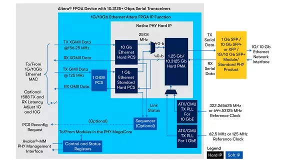
The 1G/10G Ethernet PHY Intel® FPGA Intellectual Property (IP) core supports functionality of both the standard physical coding sublayer (PCS) and the higher data rate 10G PCS with an appropriate physical medium attachment (PMA). The Standard PCS implements the 1GbE protocol as defined in Clause 36 of the IEEE 802.3 2005 Standard and also supports auto-negotiation as defined in Clause 37 of the IEEE 802.3 2005 Standard. The 10G PCS implements the 10G Ethernet protocol as defined in the IEEE 802.3 2005 standard.

The user can switch dynamically between the 1G and 10G PCS using the Intel® FPGA Transceiver Reconfiguration Controller IP core to reprogram the core. This IP core targets 1G/10GbE applications including network interfaces to 1G/10GbE dual speed SFP+ pluggable modules, 1G/10GbE 10GBASE-T copper external PHY devices to drive CAT 6/7 shielded twisted-pair cables and chip-to-chip interfaces.
Key features

  • Integrated SGMII / 1000BASE-X / 10GBASE-R (10M-10Gb) Ethernet PCS and PMA.
  • Direct internal interface with Intel® FPGA 1G/10GbE (10M-10GbE) MAC for a complete single-chip solution.
  • User selectable 1G/10Gb data rates during runtime or automatic speed detection (parallel-detect) between 1Gb and 10Gb and reconfiguration by PHY IP, or data rate selection among 10/100/1000Mb with Ethernet auto-negotiation function.
  • 10Gb, 1G/10GbE, and 10M-10GbE (SGMII/1G/10GbE) options.
  • IEEE 1588 v2 option.
  • Synchronous Ethernet (Sync-E) option.
    • Serial transceiver clock and data recovery (CDR) recovered clock output signal exposed to the FPGA fabric for routing to a Sync-E jitter cleaner phase-locked loop (PLL).
    • Separate transmitter (TX) and receiver (RX) serial transceiver PLL reference clock inputs to allow optional external Sync-E jitter cleaner PLL to feed the cleaned clock to TX PLL reference clock input.
  • Receiver-link fault status detection.
  • Local serial loop-back from transmitter to receiver at serial transceiver for self-test.
  • High-performance internal system interfaces.
    • GMII and single data rate (SDR) XGMII interfaces to 1G/10GbE (10M-10GbE) MAC, 8 bits at 125 MHz, and 72 bits at 156.25 MHz respectively for data transfer.
    • Intel® FPGA Avalon® Memory-Mapped (Avalon-MM) 32 bit interface for slave management.

Block Diagram

Specifications

Identity

Part Number
1G/10Gb Ethernet PHY Intel® FPGA IP
Vendor
Altera
Type
Silicon IP

Files

Note: some files may require an NDA depending on provider policy.

Provider

HQ: USA

Learn more about Single-Protocol PHY IP core

UFS Goes Mainstream

UniversalFlash Storage (UFS) was created for mobile applications and computer systems requiring high performance and low power consumption. These systems typically use embedded Flash based on the JEDEC standard eMMC. UFS was defined by JEDEC as the evolutionary replacement for eMMC offering significantly higher memory bandwidth. The standard builds on existing standards such as the SCSI command set, the MIPI Alliance M-PHY and UniPro as well as eMMC form factors to simplify adoption and development.

Design IP Faster: Introducing the C~ High-Level Language

In this paper, we introduce a new high-level, dataflow programming language called C~ (“C flow”) that further increases productivity by raising the level of abstraction from behavioral descriptions, while overcoming the limitations of C for hardware design. We present the syntax and semantics of this language, and the framework that provides hardware and software code generation. This paper illustrates the benefits of using C~ for hardware design of a IEEE 802.3 MAC, synthesized for FPGA and for 90nm CMOS technology.

Universal Flash Storage: Mobilize Your Data

Universal Flash Storage (UFS) was created for mobile applications and computer systems requiring high performance and low power consumption. These systems typically use embedded Flash based on the JEDEC standard eMMC. UFS was defined by JEDEC as the evolutionary replacement for eMMC offering significantly higher memory bandwidth. The standard builds on existing standards such as the SCSI command set, the MIPI Alliance M-PHY and UniProSM as well as eMMC form factors to simplify adoption and development.

Can MIPI and MDDI Co-Exist?

Since MIPI and MDDI standards both target interfaces to cameras and displays on mobile devices, are two separate standards really needed?

Frequently asked questions about Single-Protocol PHY IP

What is 1G/10Gb Ethernet PHY Intel® FPGA IP?

1G/10Gb Ethernet PHY Intel® FPGA IP is a Single-Protocol PHY IP core from Altera listed on Semi IP Hub.

How should engineers evaluate this Single-Protocol PHY?

Engineers should review the overview, key features, supported foundries and nodes, maturity, deliverables, and provider information before shortlisting this Single-Protocol PHY IP.

Can this semiconductor IP be compared with similar products?

Yes. Buyers can compare this product with similar semiconductor IP cores or IP families based on category, provider, process options, and structured technical specifications.

×
Semiconductor IP