A Process-Aware Hybrid Si/IGO Monolithic-3D 6T SRAM with BEOL Pass-Gates for the 2nm Node
By Po-Chuan Wang 1, Dongwon Jang 1, Eknath Sarkar 1, Alexei Svizhenko 2, Md. Nahid Haque Shazon 1, Piyush Kumar 1, Suman Datta 1, and Azad Naeemi 1
1 School of Electrical and Computer Engineering, Georgia Institute of Technology, Atlanta, GA 30332, USA.
2 Synopsys, Sunnyvale, CA 94085, USA.
Abstract
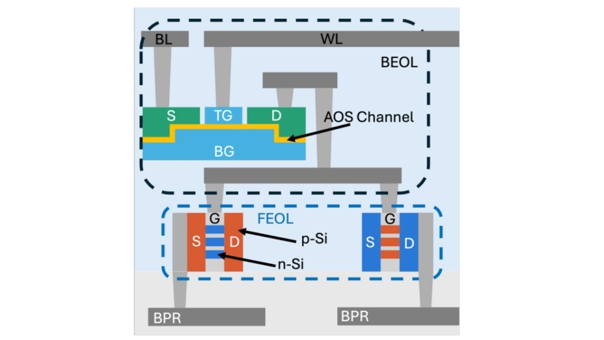
We propose a monolithic-3D (M3D) 6T SRAM at the 2nm node, integrating BEOL IGO pass-gates (PGs) with an all-silicon nanosheet latch, buried power rails (BPRs), and Ru interconnects. TCAD calibrated to a state-of-the-art double-gate IGO transistor with a tri-layer HfO₂/ZrO₂/HfO₂ (HZH) gate stack is combined with virtual fabrication and 3D parasitic extraction to realize the first process-aware layout of this topology. A novel neighbor-cell shared source/drain (S/D) bitline (BL) design enlarges the IGO contact area to mitigate contact resistance and restore PG drive without area penalty. The resulting cell achieves a 25% footprint reduction vs the high-performance (HP) 122 Si baseline while maintaining robust static noise margin (SNM) over a wide supply voltage range. At the 128×256 subarray-level, it reduces write delay by 42.2% and EDP by 9.7% compared to the high-density (HD) 111 Si baseline, owing to reduced cell parasitics and wordline (WL) loading from the smaller footprint.
To read the full article, click here
Related Semiconductor IP
- Duet Package of Embedded Memories and Logic Libraries for UMC (40nm, 28nm)
- Duet Package of Embedded Memories and Logic Libraries for TSMC (65nm, 40nm, 28nm, 16nm, N7, N6, N5, N4P)
- Duet Package of Embedded Memories and Logic Libraries for SMIC (65nm, 40nm)
- Duet Package of Embedded Memories and Logic Libraries for Huali (55nm, 40nm)
- Duet Package of Embedded Memories and Logic Libraries for GF (55nm, 40nm, 22nm)
Related Articles
- SRAM soft errors cause hard network problems
- Opto-electronics -> Hybrid integration: Production ready
- Hybrid process converts FPGAs to structured ASICs
- Hybrid Change Makes WLAN QoS Come to Life
Latest Articles
- Terracotta: Enabling the Adoption of New DRAM Techniques via a Flexible DRAM Interface and Memory Controller
- A Framework for Accelerating Transformer Inference on RISC-V for Edge AI
- An Interleaved Parallel Dependent Quantization Hardware Architecture for H.266/VVC
- A Formal Security Analysis of CAN XL
- A Secure dToF LiDAR SoC with Dual-Domain Fingerprinting and Event-Driven AFE Circuit Achieving Sensor-Level Attack Resilience