TSMC’s 3-nm Ramp Looks Different in Historical Context
By Ron Honig, EE Times | September 30, 2026
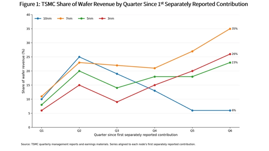
TSMC’s 3-nm process is approaching an important milestone. In the second quarter of 2026, it accounted for 30% of wafer revenue, just behind 5 nm at 33%. Recent industry reports suggest that 3 nm could become TSMC’s largest revenue-generating process family during the second half of the year.
But its current size does not tell us how quickly it got there. To compare ramp speed, I used TSMC’s quarterly disclosures to track each node’s share of wafer revenue over its first six quarters as a separate line item, for 10 nm, 7 nm, 5 nm, and 3 nm. Aligning the nodes by age, not calendar date, makes the ramps directly comparable.
To read the full article, click here
Related Semiconductor IP
- 12-bit, 400 MSPS SAR ADC - TSMC 12nm FFC
- 3.3V Capable GPIO on TSMC 28nm RF HPC+
- 1.2V Thin Oxide GPIO on TSMC 28nm RF HPC+
- LDO Voltage Regulator, 250 mA, TSMC N3P
- LDO Voltage Regulator, Adjustable 0.45 V to 0.9 V Output, 30 mA, TSMC N3P
Related News
- TSMC 3-nm Upgrade in Japan to Catch up With Demand
- GUC Announces Successful Launch of Industry's First 32G UCIe Silicon on TSMC 3nm and CoWoS Technology
- Analog Bits to Demonstrate IP Portfolio on TSMC 3nm and 2nm Processes at TSMC 2025 Technology Symposium
- TSMC looks to 5nm MRAM, plans first European design centre
Latest News
- Arm Comments on Jury Decision in Qualcomm Trial
- Alliance for Open Media Sees Rapid AV2 Adoption Across the Video Ecosystem Just Four Months After Release
- Rambus and ChipAgents Collaborate to Accelerate Chip Design with Agentic AI
- Server CPU Shipments Projected to Grow Over 40% YoY in 2027, with Arm-Based Products Continuing to Gain Market Share
- UMC and AP Memory Collaborate to Enable Advanced Power Delivery Solutions for AI and HPC Systems