TSMC 3-nm Upgrade in Japan to Catch up With Demand
By Alan Patterson, EE Times | February 10, 2026
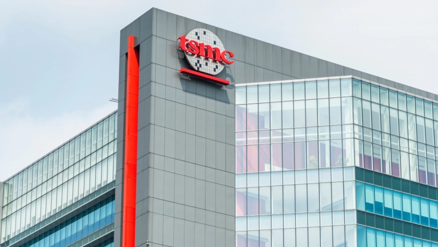
TSMC’s plan to upgrade its existing facilities in Japan to 3-nm node is aimed at catching up with strong AI demand in both domestic and global markets, analysts told EE Times.
TSMC CEO C.C. Wei announced the decision during a televised meeting with Japanese Prime Minister Sanae Takaichi. The foundry will transfer its 3-nm manufacturing process technology to its second fab near the southern city of Kumamoto, which was originally designed to produce 6-nm chips.
TSMC is upgrading in Japan as the company struggles to keep pace with demand. The company has budgeted a record $52 to $56 billion for capital expenditures this year, an increase of as much as 37% compared with 2025. TSMC hinted that it will continue to ramp up investment over the next three years. While the company didn’t disclose the size of the planned investment in Japan, analysts who spoke to EE Times estimated the value of the upgrade to be as much as $20 billion.
To read the full article, click here
Related Semiconductor IP
- 12-bit, 400 MSPS SAR ADC - TSMC 12nm FFC
- 3.3V Capable GPIO on TSMC 28nm RF HPC+
- 1.2V Thin Oxide GPIO on TSMC 28nm RF HPC+
- LDO Voltage Regulator, 250 mA, TSMC N3P
- LDO Voltage Regulator, Adjustable 0.45 V to 0.9 V Output, 30 mA, TSMC N3P
Related News
- GUC Announces Successful Launch of Industry's First 32G UCIe Silicon on TSMC 3nm and CoWoS Technology
- Analog Bits to Demonstrate IP Portfolio on TSMC 3nm and 2nm Processes at TSMC 2025 Technology Symposium
- Alphawave Semi Taped-Out Industry Leading 64Gbps UCIe™ IP on TSMC 3nm for the IP Ecosystem, Unleashing Next Generation of AI Chiplet Connectivity
- ParthusCeva announces extensive upgrade to PLLXpert online and the addition of TSMC 0.13um PLL Compilers
Latest News
- GF unveils roadmap to deliver the world’s most advanced FD-SOI platform for Physical AI
- GlobalFoundries marks Dresden expansion milestone, announces next-generation platform for Physical AI
- TSMC September 2026 Revenue Report
- Lattice Collaborates with Arm to Advance Secure, Adaptable AI Data Center Infrastructure
- ZLG Selects CAST CAN XL and TSN IP for Next-Generation Vehicle-Network Development and Test Tools