Overview
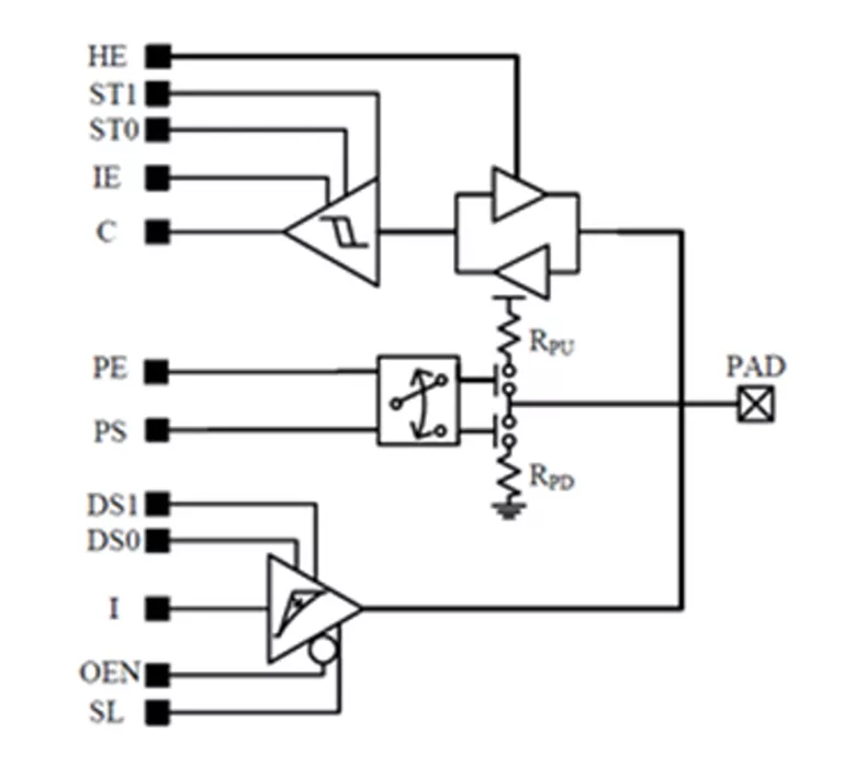
The 1.2V Thin Gate GPIO is an IP macro for on-chip integration. It is a 1.2V general purpose I/O that does not rely on thick-gate devices. Only thin-gate, 0.9V capable core MOS devices are used in the design.
Supported features include core isolation, programmable slew rate compensation, programmable drive strength, input/output enable, pull select and pull enable. Extra features such as programmable hysteresis can be supported upon request.
The 1.2V Thin Gate GPIO targets radiation hard applications or other applications prohibiting the use of thick gate I/O devices. By default, a 2kV HBM ESD protection is included. This is however easily scaled to any desired level. This specific IP macro is designed in TSMC 28nm RF HPC+, and can be ported to other technologies upon request using Sofics inhouse design tool flow.
Physical implementation
- TSMC 28nm RF HPC+ 1P9M
- No thick gate devices, MIM cap or STI required
- Pad size 70um x 70um
Learn more about GPIO IP core
Most practical photonic systems combine a Photonic Integrated Circuit (PIC), which manipulates photons, with an Electronic Integrated Circuit (EIC) that manipulates electrons. Both types of chips require highly specialized design expertise and dedicated manufacturing processes. Both must also ultimately work together seamlessly. And both can take considerable time and engineering effort to develop from scratch. The best approach for such a design task is to start from proven IP on both sides. Alcyon Photonics and Sofics bring complementary expertise to this challenge.
Specialty I/O topologies, co-designed with robust on-chip ESD protection, give SoC and chiplet designers expanded interface voltage, and I²C options on advanced processes
We joined Siemens EDA, through EDA Solutions in June 2026 for a webinar on why a design that looks perfectly correct on schematic can still fail once it’s extracted from layout, and what that means for specialty I/O verification at advanced nodes.
Most chips live an easy life with room temperature, clean power and a steady supply. The chips in this article do not. They sit inside nuclear reactors, ride on satellites and work next to particle beams, where a single stray particle can corrupt data or destroy a device.
To complete our task as engineers we rely on the tools we use. We collaborated with Siemens EDA solutions back in 2025 on a webinar about how we use their tools to develop our designs and layouts.
Collaboration brings together robust ESD protection for electrical ICs and foundry-validated IP for photonic ICs, helping mutual customers accelerate photonics product development.