NIST and Google to Create New Supply of Chips for Researchers and Tech Startups
Cooperative research agreement aims to unleash innovation in the semiconductor and nanotechnology industries.
GAITHERSBURG, Md. — September 15, 2022 -- The U.S. Department of Commerce’s National Institute of Standards and Technology (NIST) has signed a cooperative research and development agreement with Google to develop and produce chips that researchers can use to develop new nanotechnology and semiconductor devices.
The chips will be manufactured by SkyWater Technology at its Bloomington, Minnesota, semiconductor foundry. Google will pay the initial cost of setting up production and will subsidize the first production run. NIST, with university research partners, will design the circuitry for the chips. The circuit designs will be open source, allowing academic and small business researchers to use the chips without restriction or licensing fees.
Large companies that design and manufacture semiconductors often have ready access to these types of chips. But the cost can run into the hundreds of thousands of dollars, presenting a major hurdle to innovation by university and startup researchers. By increasing production to achieve economies of scale and by implementing a legal framework that eliminates licensing fees, the collaboration is expected to bring the cost of these chips down dramatically.
“By creating a new and affordable domestic supply of chips for research and development, this collaboration aims to unleash the innovative potential of researchers and startups across the nation,” said Under Secretary of Commerce for Standards and Technology and NIST Director Laurie E. Locascio. This collaboration was planned before the recent passage of the CHIPS Act, but, Locascio said, “This is a great example of how government, industry and academic researchers can work together to enhance U.S. leadership in this critically important industry.”
Modern microelectronic devices are made of components that are stacked like layers in a cake, with the bottom layer being a semiconductor chip. The NIST/Google collaboration will make available a bottom-layer chip with specialized structures for measuring and testing the performance of the components placed on top of it, including new kinds of memory devices, nanosensors, bioelectronics and advanced devices needed for artificial intelligence and quantum computing.
NIST anticipates designing as many as 40 different chips optimized for different applications. Because the chip designs will be open source, researchers will be able to pursue new ideas without restriction and share data and device designs freely.
“This is a great example of how government, industry and academic researchers can work together to enhance U.S. leadership in this critically important industry.” —Under Secretary of Commerce for Standards and Technology and NIST Director Laurie E. Locascio
"Google has a long history of leadership in open-source,” said Will Grannis, CEO of Google Public Sector. “Moving to an open-source framework fosters reproducibility, which helps researchers from public and private institutions iterate on each other’s work. It also democratizes innovation in nanotechnology and semiconductor research.”
The SkyWater foundry will produce the chips in the form of 200-millimeter discs of patterned silicon, called wafers, which universities and other purchasers can dice into thousands of individual chips at their own processing facilities.
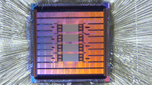
This NIST-developed chip is used to measure the performance of memory devices used by artificial intelligence algorithms. NIST and Google have signed a cooperative research and development agreement to produce a new suite of chips for measuring the performance of devices used in a range of advanced applications.
The 200mm wafer is an industry standard format compatible with the manufacturing robots at most semiconductor foundries. Giving researchers access to chips in this format will allow them to prototype designs and emerging technologies that, if successful, can be integrated into production more quickly, thus speeding the transfer of technology from lab to market.
Research partners contributing to the chip designs include the University of Michigan, the University of Maryland, George Washington University, Brown University and Carnegie Mellon University.
NIST will host a virtual workshop Sept. 20-21, 2022, on the use of chips for measurement science and prototyping. The workshop will include a working group meeting on the NIST/Google collaborative research and development agreement that will be open to public participation. Information and registration instructions are available on the NIST website.
Related Semiconductor IP
- NPU IP
- JPEG XL Encoder
- I2C Master/Slave Controller Core
- NVMe Validation Test Suite
- Hybrid Memory Cube Verification IP
Related News
- SkyWater to Provide Foundry Service for new NIST and Google Partnership to Create Supply of Chips for Researchers and Tech Startups
- Chip Interfaces Appoints Avant Technology as one of its distributors for Taiwan and China to Expand Business Opportunities in the IP Market
- Arteris Wins Funding to Expand Hardware Design Supply Chain Security Assurance for the Trusted and Assured Microelectronics Program
- onsemi to Acquire Synaptics to Enable the Next Generation of Intelligent Systems for Physical AI
Latest News
- GF unveils roadmap to deliver the world’s most advanced FD-SOI platform for Physical AI
- GlobalFoundries marks Dresden expansion milestone, announces next-generation platform for Physical AI
- TSMC September 2026 Revenue Report
- Lattice Collaborates with Arm to Advance Secure, Adaptable AI Data Center Infrastructure
- ZLG Selects CAST CAN XL and TSN IP for Next-Generation Vehicle-Network Development and Test Tools