Imec demonstrates the first 3D implementation of a charge coupled device for AI memory applications
The feasibility of processing a charge coupled device (CCD) in a 3D NAND-like architecture paves the way for a cost-effective, high-bit-density memory solution to address the memory wall for AI specific workloads
LEUVEN (Belgium) — May 12, 2026 — This week, at the 2026 IEEE International Memory Workshop (IMW), imec, a world-leading research and innovation hub in advanced semiconductor technologies, presents a 3D implementation of a CCD memory device with IGZO channel – a world first. The functional 3D CCD device consists of vertical memory holes drilled through a stack of 3 word-lines, serving as phase gates. Transfer of charges (that make up the bits) across the gates could be demonstrated at >4MHz transfer speed. The feasibility of processing the CCD device in a 3D NAND Flash architecture ensures cost-effective fabrication and bit densities surpassing the DRAM limit. This makes the block-addressable 3D CCD device an attractive compute express link (CXL® ) type-3 buffer memory for AI use cases – designed to feed multiple processors with large blocks of data through a high-bandwidth CXL® switch.
AI’s insatiable hunger for memory is putting significant pressure on DRAM-based memory technology, which increasingly struggles to maintain the cost-per-bit scaling trendline. The memory industry therefore explores alternative, more cost-effective memory solutions that can complement DRAM and DRAM-based high bandwidth memory (HBM) for AI-specific workloads. In parallel, new memory interfaces have emerged that allow for more efficient use of the main memory resources compared to traditional double data rate (DDR) buses. One of these is CXL®, a memory protocol designed to make large pools of memory available to multiple processors through a high-bandwidth CXL® switch. These so-called CXL® type-3 buffer memories have different specifications than DRAM, offering an excellent opportunity for the introduction of new memory technology.
In 2024, imec conceptually introduced the 3D CCD with an IGZO channel – offering promising prospects to be used as a CXL® type-3 buffer memory – and demonstrated memory operation on a 2D proof-of-concept. Maarten Rosmeulen, Program Director Storage Memory at imec: “The potential of this CCD device to be used as a buffer memory lies in its ability to be integrated in a 3D NAND Flash string architecture – the most cost-effective way to achieve a scalable, high bit density estimated to go far beyond the DRAM limit. We now show for the first time a functional 3D implementation with a 3-word-line structure, achieving vertical IGZO channels at dimensions comparable with what can be achieved for 3D NAND (i.e., 80-120nm diameter memory holes).”
In the 3D device, the CCD registers – or strings – are integrated into vertically aligned plugs, which are drilled through the 3-word-line stack using a 3D NAND-inspired punch-and-plug process. The horizontal word-lines act as the gates and determine a series of bits in each string. These bits are based on charges, which can be serially transferred and stored across the gates using a pulsed voltage scheme.
“We achieve reliable charge transfer along the vertical IGZO channel at speeds exceeding 4MHz,” adds Maarten Rosmeulen. “The number of charges transferred per cycle was measured to be a few thousand, which is sufficient for one bit or even multibit storage in real memory applications. Unlike byte-addressable DRAM, our 3D CCD device is designed to provide block-level data access, which is better suited to modern AI workloads. These results, in combination with unlimited endurance, long data retention (ensured by the IGZO channel material), and low-voltage operation (due to the charge-based nature of the memory operation) bring the 3D CCD technology a step closer to buffer memory implementations. In ongoing work, we focus on expanding the number of word-lines and optimizing the readout stage of our 3D CCD buffer memory. We are now ready to take our 3D CCD device technology to the next level with industry partners and fully unlock its potential for AI memory applications.”
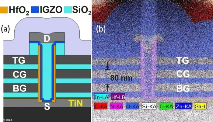
Figure 1 – (a) Schematic of the 3-word-line based 3D CCD structure: bottom gate (BG), center gate (CG), and top gate (TG), with source (S) at the bottom and drain (D) at the top; (b) cross-sectional TEM image showing 3 gate layers with a word-line pitch of 80nm.
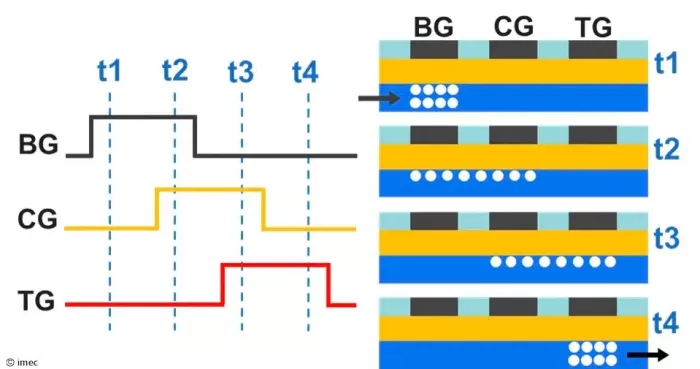
Figure 2 – (a) Illustration of the pulsing scheme across 3 gates for serial charge transfer in a 3-word-line based 3D CCD memory; (b) Schematic of 3D CCD operation showing electron transfer through the formation and shifting of potential wells under the gates.
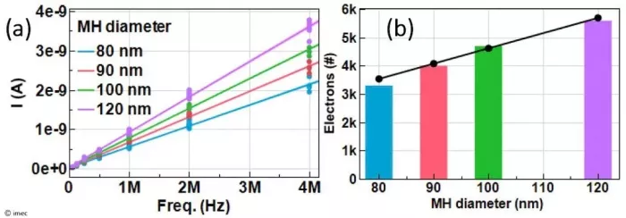
Figure 3 – (a) I-f characteristics from 7 devices with varying memory hole (MH) diameters, measured up to 4MHz; (b) the number of electrons transferred per cycle obtained from the slope of the corresponding I-f curves.
About imec
Imec is a world-leading research and innovation hub in advanced semiconductor technologies. Leveraging its state-of-the-art R&D infrastructure and the expertise of over 6,500 employees, imec drives innovation in semiconductor and system scaling, artificial intelligence, silicon photonics, connectivity, and sensing.
Imec’s advanced research powers breakthroughs across a wide range of industries, including computing, health, automotive, industry, consumer electronics, aerospace and security. Through IC-Link, imec guides companies through every step of the chip journey - from initial concept to full-scale manufacturing - delivering customized solutions tailored to meet the most advanced design and production needs.
Imec collaborates with global leaders across the semiconductor value chain, as well as with technology companies, start-ups, academia, and research institutions in Flanders and worldwide. Headquartered in Leuven, Belgium, imec has research facilities in Belgium, across Europe, the USA and the GCC region, and representation on three continents. In 2025, imec reported revenues of €1.2 billion.
For more information, visit www.imec-int.com
Related Semiconductor IP
- DSP-Based 112G SerDes
- XTAL oscillator in TSMC-7nm
- GPU
- V-by-One Verification IP
- AI model compression IP
Related News
- Imec Teams With Cadence to Present Automated Design-for-Test (DFT) Solution for 3D Memory-on-Logic
- Spansion and XMC Expand Partnership to Jointly Develop 3D NAND
- Micron and Intel Unveil New 3D NAND Flash Memory
- Mobiveil Announces FPGA-Based SSD Platform for 3D NAND Flash Devices, Upgrades NVMe, PCI Express Controllers to Support Latest Specifications
Latest News
- Arteris Deployed by Speedata for Data Center Compute
- Siemens to acquire Defacto Technologies to complement its EDA portfolio with automated SoC design creation
- Mach42 Completes £7M Funding Round, Led by IP Group With Investment From BGF and Foresight Group
- ELECTRA IC Unveils Comprehensive IP Core Suite for Next-Generation Post-Quantum Cryptography
- CAST Enhances Serial Memory Controller IP with Encryption, Low-Power, and ASIL-Ready Options