Development of High-Precision Nonvolatile Analog Computing-in-Memory Technology Enabling Ultra-Low-Power AI Hardware
May 12, 2026
Key Highlights
- Floadia Corporation (hereinafter “Floadia”), NEC Corporation, and National University Corporation Kyushu Institute of Technology (hereinafter “Kyushu Institute of Technology”) have jointly developed high-precision programming and long-term retention technologies for AI model parameters of Nonvolatile Analog Computing-in-Memory (nvACiM), next-generation hardware capable of ultra-low-power AI inference.
- Conventional nvACiM memory faced challenges such as large variations in programming speeds, which limited the number of parameter levels (bit accuracy) per memory cell, and parameter drift over time, both leading to reduced inference accuracy.
- By utilizing SONOS-type flash memory and an iterative multi-step programming sequence with optimal voltages, the team achieved high-precision setting of multilevel parameters within a single memory cell. In addition, long-term parameter retention was realized through a specialized thermal treatment to optimize the band structure of the charge storage layer of the SONOS memory cell and a process to remove unstable electrons during programming sequence.
- These technologies improve nvACiM calculation accuracy, contributing to higher performance, energy efficiency, and miniaturization of edge AI devices such as robots, drones, and automobiles.
Background
AI technologies using GPUs, such as large language models and image recognition, are transforming our lives. However, GPU-based inference relies on digital computation, requiring high-performance computation by processors and repeated high-speed data transfers of input data and parameters (weights) between the processors and memories, consuming significant power. Nonvolatile Analog Computing-in-Memory (nvACiM) technology enables ultra-low-power AI processing by pre-setting parameters in multiple memory cells and performing multiply-accumulate (MAC) operations in parallel as analog data is input.
Despite its potential, conventional nvACiM memories suffered from significant programming speed variations between memory cells, limiting the number of parameter levels (bit precision) in each memory cell. Furthermore, parameter values shifted over time. These characteristics degraded inference accuracy. Consequently, there was an urgent need for technology that could both precisely program multi-level parameters and retain them over long periods (Fig. 1).
Technical Details
- Application of SONOS Memory
The team utilized Floadia’s foundry-proven SONOS-type flash memory technology for nvACiM. SONOS memory stores data by accumulating electrons in discrete traps in a silicon nitride film, which theoretically allows for the setting of parameters with high bit accuracy. Advantages of SONOS memory include low programming speed variation between memory cells and high electron retention. However, previous reports from other institutes were limited to only 8-level programming per cell (3-bit precision).
- High-Precision Parameter Programming Technology
To achieve high bit precision, the team developed an “iterative multi-step programming sequence”. This method divides the programming into multiple steps, repeating “program and verify” cycles using optimal voltages for specific parameter values and doubling the number of parameter levels in each step. Simulations confirmed that 256 levels (8-bit precision) could be set within a range of 4 to 1024 nA.
- Long-Term Parameter Retention Technology
While SONOS memory has superior retention, nvACiM requires even higher stability due to the small current differences between parameter levels. The team developed:
Band Control Thermal Treatment (BCT): A specialized heat treatment during storage-layer formation that optimizes the band structure to suppress electron leakage while keeping programming voltages low.
Shallow Trap Charge Reduction (STR) Process: A process implemented into the programming sequence to remove electrons trapped in “shallow” levels, which are prone to escaping and causing parameter drift.
These advancements enabled long-term parameter retention.
- Verification Using nvACiM Test Chip
The technologies were implemented and verified on a test chip. 32 parameter levels (5-bit precision) were successfully set in 2 nA increments between 2 and 64 nA. The average standard deviation of the parameter distribution was 0.78% (Fig. 2). These results surpassed the previously reported best of 3 nA increments between 3 and 100 nA with 1.3% standard deviation for floating-gate flash memory, which realizes ultra-low-power inference. High-precision MAC operations were also confirmed successfully.
This work is based on results obtained from a project, JPNP16007, commissioned by the New Energy and Industrial Technology Development Organization (NEDO).
The technologies were presented at International Memory Workshop (IMW) 2026, which was held in Leuven, Belgium from May 10th to 13th.
Explore Flash IP:
Conference information
Conference name: IEEE International Memory Workshop (IMW) 2026
Dates: May 10th to 13th, 2026
Title: Enhancing SONOS-type Flash Memory for Nonvolatile Analog Computing-in-Memory via Precise Multi-level Weight Control and Improved Retention
Authors: T. Kobayashi, Y. Taniguchi, H. Ikegaya, T. Tamatsu, M. Yamaguchi, K. Yanagisawa, Y. Uji, T. Yabe, S. Yoshida, Y. Kawashima, T. Shimozato, H. Kobori, T. Kato, F. Owada, S. Noda, H. Yoneda, K. Okuyama, T. Hosomi, K. Oto, S. Koshina, T. Morie
URL:https://ewh.ieee.org/soc/eds/imw/
For inquiries regarding this press release;
Floadia: https://floadia.com/jp/#contact
Kyushu Institute of Technology: Takashi Morie, Ph.D., Special Appointed Professor, Research Center for Neuromorphic AI Hardware (morie@brain.kyutech.ac.jp)
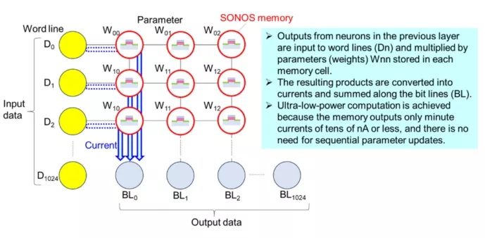
Fig. 1. Operating principle of Nonvolatile Analog Computing-in-Memory (nvACiM).
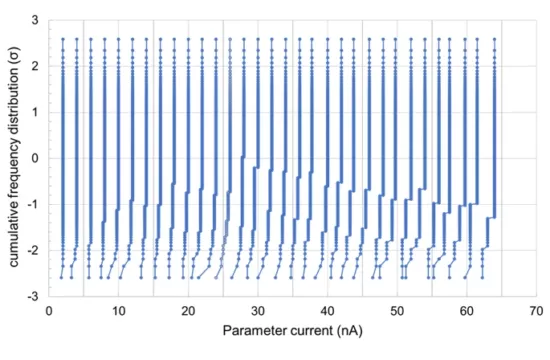
Fig. 2. Results of 32-level parameter setting in 2 nA increments obtained from the nvACiM test chip.
Related Semiconductor IP
- Flash Beyond Flash IP
- SPI/SPANSION FLASH Verification IP
- SPI/SERIAL FLASH Verification IP
- SPI (Serial Peripheral Interface) Flash Verification IP
- Serial Flash Verification IP
Related News
- Computing-in-Memory Innovator Solves Speech Processing Challenges at the Edge Using Microchip's Analog Embedded SuperFlash Technology
- Toshiba and Japan Semiconductor Develop Highly Reliable Versatile Analog Platform with Floadia's G1 technology for Automotive Applications
- Taiwan Industrial Technology Research Institute (ITRI) to Build Semiconductor IP Delivery and Design Management Systems using D&R's IP Manager Series(tm)
- Sony Semiconductor Kyushu Selects Artisan Library Solutions
Latest News
- Arteris Deployed by Speedata for Data Center Compute
- Siemens to acquire Defacto Technologies to complement its EDA portfolio with automated SoC design creation
- Mach42 Completes £7M Funding Round, Led by IP Group With Investment From BGF and Foresight Group
- ELECTRA IC Unveils Comprehensive IP Core Suite for Next-Generation Post-Quantum Cryptography
- CAST Enhances Serial Memory Controller IP with Encryption, Low-Power, and ASIL-Ready Options