EnSilica Establishes New Engineering Hub in Cambridge
May 28, 2025 -- EnSilica, a leading chip maker of mixed signal ASICs (Application Specific Integrated Circuits), is pleased to announce that it has established a new engineering hub in Cambridge, UK.
Drawing on Cambridge’s renowned semiconductor ecosystem, EnSilica has opened a new engineering facility in the city and has recruited six engineers, four of whom hold PhDs, thereby increasing the company’s global workforce to 190.
With the addition of this new facility and technical expertise, EnSilica will expand its existing mmWave / RF integrated circuit design capabilities, an area in which the Company has already seen significant customer demand. The expansion has been facilitated by the recent UK Space Agency C-LEO funded award, alongside additional contract momentum and customer wins that continue to support the Company’s growth.
EnSilica currently operates across three UK engineering design centres in Abingdon, Sheffield and Bristol, alongside additional international engineering facilities in Bangalore, India, and Porto Alegre and Campinas in Brazil.
Ian Lankshear, Chief Executive Officer of EnSilica, commented: “We are delighted to have not only secured a team of highly skilled engineers at a time when there is a very real shortage of engineering talent in the UK, but also to establish a firm base in an established UK tech hub like Cambridge which ideally positions the business to attract additional talent.
By further expanding our engineering knowhow across the satellite and communications market, I believe that this investment will enable the business to capitalise further on very real and near-term growth opportunities.”
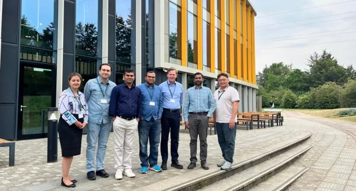
Figure 1: EnSilica staff outside the new Cambridge facility
About EnSilica
EnSilica is a leading fabless design house focused on custom ASIC design and supply for OEMs and system houses, as well as IC design services for companies with their own design teams. The company has world-class expertise in supplying custom RF, mmWave, mixed signal and digital ICs to its international customers in the automotive, industrial, healthcare and communications markets. The company also offers a broad portfolio of core IP covering cryptography, radar, and communications systems. EnSilica has a track record in delivering high quality solutions to demanding industry standards. The company is headquartered near Oxford, UK, and has design centres across the UK and in India and Brazil.
Related Semiconductor IP
- UALink 200G v1.0 Verification IP
- CCSDS SCCC Demapper and Turbo Decoder
- NPU IP
- JPEG XL Encoder
- I2C Master/Slave Controller Core
Related News
- Agile Analog to move into iconic Radio House office block in Cambridge, UK to enable significant increase in engineering staff
- Arteris Opens New Engineering Hub in Poland
- Baya Systems Expands Bengaluru Engineering Hub to Scale AI, Automotive and HPC Innovation
- Cadence Completes Acquisition of Hexagon’s Design and Engineering Business, Advancing Leadership in Physical AI and Multiphysics
Latest News
- Marvell, Microsoft and Oracle Establish OCP Working Group to Standardize Data Center Hardware Security
- At GAITA, PUFsecurity Shows How PUFrt and PUF-Based HSMs Give Agentic and Physical AI a Verifiable Root of Trust
- QuickLogic Secures Six-Figure eFPGA IP Contract for Automotive Industrial SoC
- Faraday Powers Intelligent Sensing with New 14nm MIPI C/D Combo PHY IP
- Cadence Wins Five 2026 TSMC OIP Partner of the Year Awards