Why schematic-correct designs fail at advanced nodes

Siemens EDA and Sofics Webinar 2026
Introduction
Getting a design to pass simulation at schematic level is only half the job.
We joined Siemens EDA, through EDA Solutions in June 2026 for a webinar on why a design that looks perfectly correct on schematic can still fail once it’s extracted from layout, and what that means for specialty I/O verification at advanced nodes. You can watch the webinar here.
Khalid Teama from EDA Solutions opened with an overview of the Siemens custom IC design flow. He focused on Calibre for physical verification and parasitic extraction, and the Solido simulation suite for post-layout verification. Rani Baetens, analog design engineer at Sofics, then walked through two real design cases where our schematic simulations looked clean, but the extracted layout told a different story. Plus a Calibre feature that makes tracking down these issues a lot less painful.
Webinar overview
The session was framed around a simple truth. A design can be fully correct at schematic level and pass every corner. It can still misbehave once layout effects, parasitics and real process conditions are folded in. For specialty I/Os, reliability, ESD robustness and performance all have to hold at once. That gap between schematic intent and post-layout reality can be the difference between a working chip and a costly respin.
Khalid’s part of the talk covered the Siemens ecosystem and how Calibre and Solido fit into the design flow. He was clear that parasitic extraction is not optional. Rani then grounded this in two Sofics designs: an over-voltage tolerant (OVT) GPIO in TSMC 22nm and a low-power voltage regulator in TSMC 4nm. These issues do not appear on schematic level design.
Siemens EDA design flow: Calibre and Solido
Khalid introduced the Siemens custom IC design platform as a full backbone flow, not a set of disconnected tools. S-Edit handles schematic capture on open access databases. The Solido design environment and simulation suite handle verification. L-Edit handles layout. Calibre handles physical verification and sign-off. A foundry enablement team maintains formal relationships with foundries, so the processes you’re targeting are already validated on the tools.
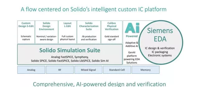
Figure 1. The Siemens EDA custom IC design platform, from schematic capture through layout to Calibre physical verification, with the Solido simulation suite at the center.
The core message on Calibre was that it’s far more than a DRC and LVS tool. It covers reliability checking through Calibre PERC and power integrity through PowerEM. It also includes shift-left products like LVS Recon and DRC Recon, which identify violations earlier in the flow before they turn into expensive late-stage changes. Calibre is the sign-off standard at all major foundries. That matters in practice: the tool you verify with is the same one the foundry uses to decide whether your design can be manufactured.
The part that connects most directly to what Rani presented afterward is parasitic extraction. Extraction reveals the real behavior of your layout, not the ideal schematic. Metal traces bring resistance and voltage drop. Capacitance slows switching and adds power. Parallel routes couple and create noise. Long wires bring inductance that shows up as ringing at high speed. Skipping this step is not a shortcut, it’s a risk. The numbers Khalid shared were blunt: 60 to 80% of timing violations only surface after extraction. Unmodeled parasitics can add: 30 to 50% to power estimates. A respin can run up to 5 million dollars depending on the node.
Calibre handles this with rule-based extraction (XRC) for nodes at 22nm and above, and field solvers (Calibre exact and exact 3D) for 16nm and below or wherever higher accuracy is needed. That includes standard cell and memory characterization, RF layouts, and non-rectangular geometries like MEMS and touchscreens. On the simulation side, the Solido suite takes those extracted parasitics and turns them into fast, accurate post-layout verification. Reported speedups run 2 to 30x faster than competing simulators.
Sofics design methodology
Rani opened her part of the talk with the methodology behind both design cases. A design phase in S-Edit is verified with the Solido simulation suite. A layout phase in L-Edit runs nmLVS and nmDRC. A final verification phase extracts the layout with Calibre xRC/xACT and re-simulates it. If an issue turns up at final verification, it loops back to the layout phase. That’s exactly what happened in both cases below in figure 2.
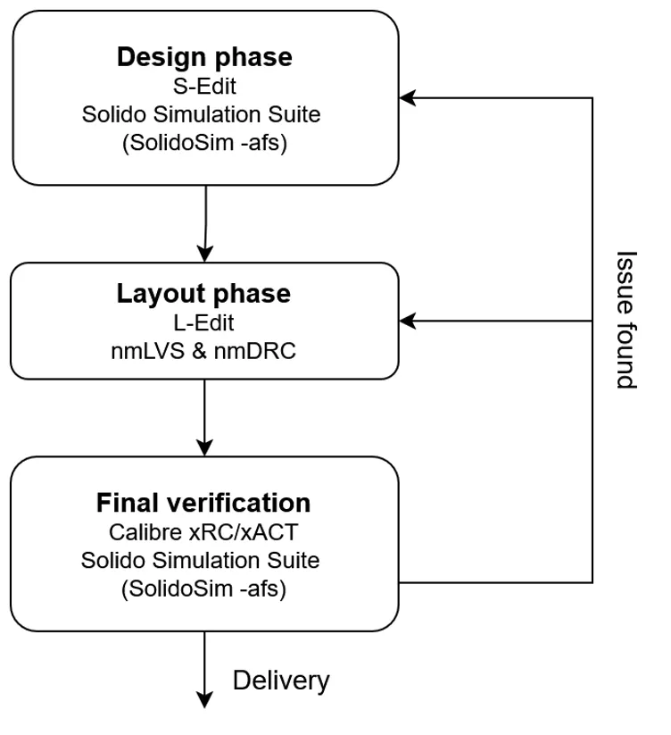
Figure 2. The Sofics design flow used for both cases below. An issue found at final verification sends the design back to the layout phase for rework.
Case 1: a GPIO that stopped switching and the well proximity effect
The first case Rani walked through was a GPIO in TSMC 22nm. It supports three supply voltages (1V, 1.2V and 1.8V, each with 10% variation) plus an additional 3.3V rail to overdrive the driver. The design included 2kV HBM ESD protection and was targeted at 25MHz for loads up to 100fF.
At schematic level, everything checked out: rise and fall times were within spec across corners and leakage was fine. Nothing stood out. But once the layout was extracted with Calibre and re-simulated, the GPIO pad stopped switching in some corners. The layout was fully DRC and LVS clean the whole time.
Tracing the waveforms pointed to a level shifter that moves a signal from the I/O domain (as low as 1V minus 10%) up to the 3.3V domain. The level shifter’s input devices have a threshold voltage that can range from 0.5V to 0.8V depending on corner. That already leaves little overdrive margin in schematic simulation. Comparing the schematic netlist to the XRC netlist showed that some device parameters had shifted, which can be observed in figure 3. That shift pushed the threshold voltage up further, to the point where the input devices never turned on and the level shifter stopped switching.
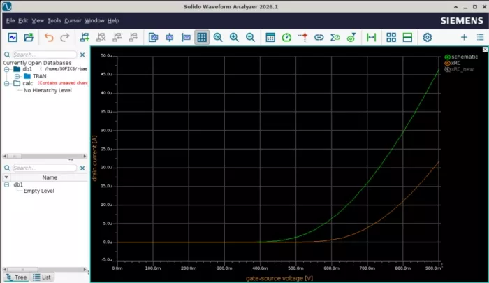
Figure 3. Drain current versus gate-source voltage for the same input device, schematic in green against the extracted XRC netlist in orange. At 0.9V gate-source voltage, the schematic device has roughly double the drive strength of the extracted one, despite an LVS-clean layout.
Digging into what had changed led to the well proximity effect. Doping concentration near a well edge in this technology shifts device characteristics like threshold voltage. The OD2 layer in this layout was drawn at minimum size, putting the device right at that edge as seen in figure 4.
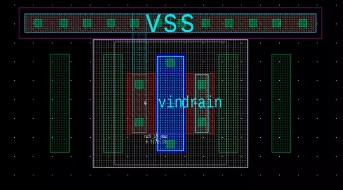
Figure 4. The layout that produced the mismatch. The OD2 layer (highlighted) is drawn at minimum size, right at the well edge, which is what triggers the well proximity effect on the device threshold voltage.
Once the cause was clear, so was one fix. Enlarge the OD2 spacing around the sensitive device, which solved the issue seen in figure 6. The extracted result moved back in line with the schematic. But it also ate up a lot of area, which we can see in figure 5. In the final design we went a different route and redesigned the level shifter itself to be robust to the well proximity effect. That ended up costing less silicon area than widening the spacing.
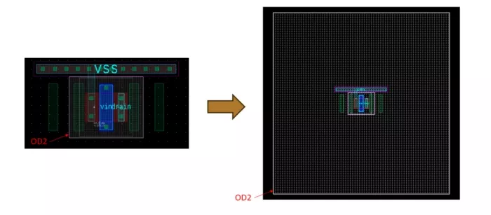
Figure 5. Widening the OD2 spacing (right) moves the device clear of the well proximity zone and restores the expected threshold voltage, at the cost of extra area. The level shifter redesign we used in production achieved the same result more compactly.
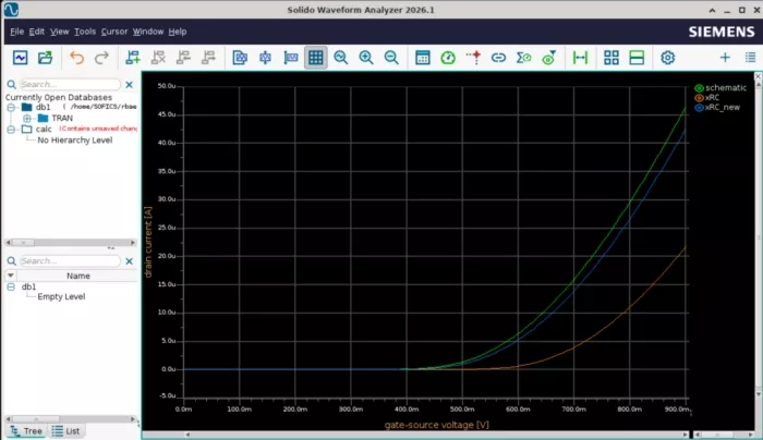
Figure 6. Simulation and extracted parameters showing the improvements of increasing the OD2 layer.
Case 2: a floating-gate dummy device and a leakage current that crept up
The second case was a low-power voltage regulator in TSMC 4nm. It generates 0.6V and 1.2V from a 1.8V supply, designed for a 1.8V GPIO in a FinFET process. Schematic simulation again looked clean, with DC leakage under 1µA. After layout and extraction the circuit still worked functionally. Output voltages were within spec and it could drive the intended loads. But DC current consumption climbed steadily to more than 20µA a big jump from what schematic predicted.
The culprit was a PODE device (poly on OD edge), effectively a recognition-layer dummy device in this FinFET technology. It had been placed in the middle of a real device rather than at the intended OD edge. Because of where it sat it behaved like an actual device with a floating gate seen in figure 6. That lowered the impedance of the path from 1.8V to ground and drove up leakage. The recognition layer meant it wasn’t flagged as a real device, so the layout stayed DRC and LVS clean throughout. The problem was invisible to standard checks.
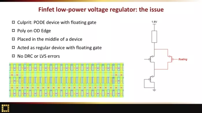
Figure 6. The PODE device (poly on OD edge) sitting inside a real device instead of at the intended edge. With its gate floating, it forms an unintended leakage path from the 1.8V rail to ground, while the recognition layer keeps the layout DRC and LVS clean.
The fix was straightforward once identified. You can connect the floating gate. Better restrict the PODE device to the OD edge where it’s intended and use real properly tied dummy gates everywhere else, shown in figure 7. We applied that second approach in a related 3.3V bias generator design, also in 4nm, generating four output voltages for one of our own over-voltage tolerant GPIOs in this technology.
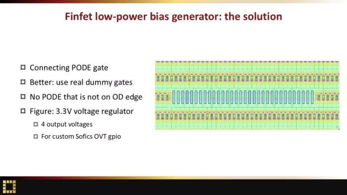
Figure 7. The fix applied in a 3.3V bias generator for a Sofics OVT GPIO: the PODE device is restricted to the OD edge, and real dummy gates are used everywhere else, removing the floating-gate leakage path.
Making sense of XRC netlists
Both cases were found by comparing waveforms and netlists between schematic and extraction. That work gets painful once a netlist runs into hundreds of thousands of lines, which is common in FinFET designs even from a schematic netlist of a few thousand. Rani highlighted a Calibre feature that helps with the PEX netlist statement. It lets you extract using schematic (source) net names instead of layout names, as long as the layout is LVS clean. This can be observed in figure 8.
The difference is significant in practice. A netlist extracted with layout names gives you fragments you can barely place a VSS pin here and an unnamed net there. The same netlist extracted with source names preserves the full hierarchy. Instances and parasitic R and C are traceable back to where they sit in the design. That turns a frustrating search into something you can actually navigate.
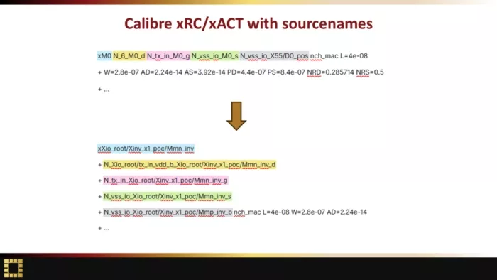
Figure 8. The same extracted netlist, once with generic layout names (top) and once with the PEX netlist source-name option (bottom). Matching colors show the same nets and devices; the source-name version keeps the full instance hierarchy, so a specific device or parasitic element is easy to find again.
Conclusion
The message from both halves of this webinar advanced nodes, schematic-correct is not the same as silicon-correct. Layout brings in effects that a clean DRC and LVS pass will not catch on its own, from well proximity to floating dummy devices to general parasitics. Extracting parasitics with Calibre and re-simulating with the Solido suite closes that gap. It’s the only reliable way to catch these issues before tape-out rather than in silicon, where a respin gets expensive fast. In both cases here getting to a fix quickly came down to being able to actually read the extracted netlist. That’s where getting familiar with features like the PEX netlist source-name option pays off.
Q&A
Several questions returned to how far Sofics pushes over-voltage tolerance.
Does TSMC N4 technology allow going as high as 3.3V?
Rani confirmed it does, though it’s not trivial. Overdrive devices in this node only tolerate 1.5V, so it takes at least a three-stack to get there. Sofics has already built a 3.3V GPIO, voltage regulator and ESD protection in this technology. It’s proven, just not easy.
How do you overcome mismatch and process variation in 22nm analog design, including local versus global effects?
Sofics designs are architected from the start to be robust across corners, Rani noted rather than tuned to a typical corner and hoping it will work everywhere. Design starts with a typical corner, but the architecture itself is what keeps mismatch and variation from becoming a problem later.
From the Siemens EDA side, Khalid fielded several product questions. Can you talk about the Calibre cloud solution?
He described Calibre Connect (Cloud Connect), which lets Calibre run on cloud or on-premise infrastructure and launch directly from third-party editors, giving design teams more flexible access to compute resources.
Is the extraction investment worth it when teams already run extensive DRC and LVS?
He was clear that DRC and LVS confirm geometric correctness and connectivity, not real electrical behavior after parasitics are introduced. Skipping extraction risks missing coupling noise, IR drop, timing degradation and signal integrity issues that only show up in silicon.
How does Calibre integrate into mixed-signal and 3D IC workflows?
He mentioned Calibre 3DStack for inter-die connectivity and verification, alongside parasitic-aware analog and digital flows and noted that matching tools to a specific design goal is best done in a direct conversation.
How is data privacy ensured in Siemens’ AI tools, given that some foundries restrict use of their data in AI tools altogether?
Khalid drew a line between the machine learning already built into tools like Solido and standalone AI products such as Siemens’ Fusion AI. Fusion AI supports on-premise deployment and a “Secure RAG” option with access controls, built specifically to address that concern.
Explore Sofics IP:
Related Semiconductor IP
Related Blogs
- Is the Role of Test Chips Changing at Advanced Foundry Nodes?
- Why Firms Fail At FPGA
- Why 6.4 Gbps DDR5 Designs Fail and How to Avoid It
- How Cadence and TSMC Are Accelerating AI Silicon Design at Advanced Nodes