UALink: Powering the Future of AI Compute

On April 25, the UALink Consortium officially released the UALink 200G 1.0 Specification, marking an important milestone with support from key hyperscalar market players. It enables a low-latency, high-bandwidth fabric that supports hundreds of accelerators in a pod and facilitates simple load-and-store semantics.
Motivation Behind UALink
The rapid evolution of Artificial Intelligence (AI) and Machine Learning (ML) is driving an unprecedented demand for high-performance computing (HPC) resources. Take the recent viral Ghibli trend, which utilizes a staggering 1 trillion floating point operations (FLOPs) to generate AI images—highlighting the computational intensity of modern workloads. These workloads require scalable interconnects optimized for high bandwidth, low latency, and efficient hardware resource utilization. While proprietary interfaces exist, the industry lacks an open standard to meet these needs. Addressing this gap, UALink emerges as the first open standard for seamless, scale-up integration of accelerators, providing a paradigm shift in AI compute space.
Quick Dive into Protocol
UALink presents a non-coherent interconnect solution, leveraging a 200G Ethernet Physical Layer (PHY) across four lanes to achieve 800 Gbps per port. Notably, the upper lanes are optimized to cater to requirements of scale-up applications.
UALink is designed as a layered protocol stack comprising four distinct, well-defined functional layers:
- Protocol layer: Simple symmetric protocol interface for data and control exchange
- Transaction layer: Defines 64B Flit packing, packet formats, and flow control mechanism
- Data Link layer: Contains error recovery features including Flit replay and RAS (Reliability, Availability, and Serviceability) features
- Physical layer: Based on 802.3dj ethernet PHY with some defined modifications
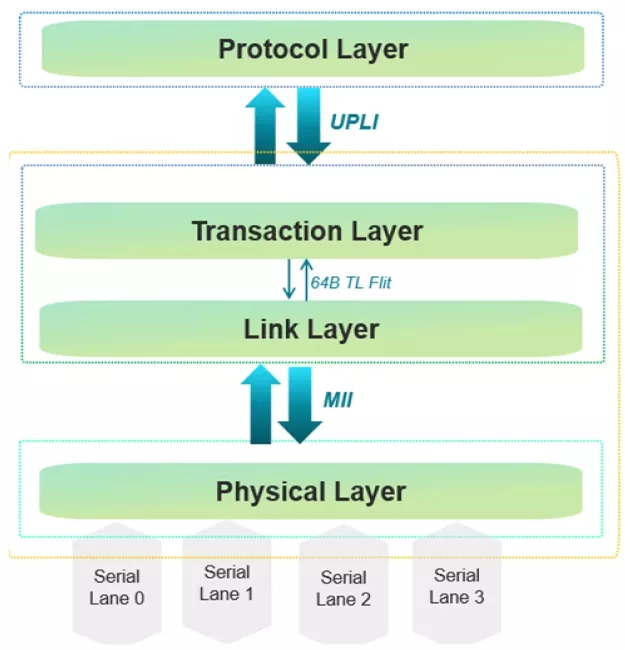
Cadence Verification IP for UALink
Cadence provides cutting-edge protocol support for the HPC and AI market, enabling our customers to be first to market with next-gen innovative solutions. Cadence VIPs is at the forefront of providing a reliable, one-stop solution for verifying AI and HPC application system-on-chips (SoCs). With proven support for PCIe 7.0, CXL 4.0, and Integrity and Data Encryption (IDE) for both PCIe and CXL, now featuring UEC and UALink VIP support, we're leading the industry in comprehensive verification offerings.
UALink VIP adheres to a layered architecture as defined by the protocol, offering flexibility to users. This modular architecture enables the utilization of the VIP at block and stack level. VIP provides callback support and error injection at logical protocol touchpoint for easy debug, coverage, scoreboarding, and other testbench requirements. Below figure shows reference verification topology with VIP.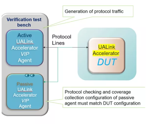
We are engaged with early adopters and looking forward to engaging with more customers as the ecosystem around UALink grows. For more information, reach out to us at <talk_to_vip_expert at cadence dot com>.
Related Semiconductor IP
- UALink PHY + Controller
- Simulation VIP for UALink
- UALink Subsystem
- UALink Controller
- UALink PCS IP Core
Related Blogs
- How Network-on-Chip Architectures Are Powering the Future of Microcontroller Design
- Rivian’s autonomy breakthrough built with Arm: the compute foundation for the rise of physical AI
- The Future of AI is Modular: Why the SiFive-NVIDIA Milestone Matters
- The Silent Guardian of AI Compute - PUFrt Unifies Hardware Security and Memory Repair to Build the Trust Foundation for AI Factories
Latest Blogs
- From Bug Hunting to Engineering Methodology: Lessons from AI-Driven Development
- Manufacturing Intelligence: Turning EDA Data into Trusted Action
- Execute-in-Place: Getting More from Embedded NVM
- Rethinking RTL flows with AI-driven hybrid formal verification
- Arm and NVIDIA: Building the trusted compute foundation for the agentic AI era