Hitting the Memory Wall:Why Cache Miss Tolerance Defines CPU Performance Now

Insights from Evaluating the FlatBuffers Workload on Andes RISC-V
The memory wall is no longer a theoretical concern. It is the defining bottleneck in today’s AI, automotive, and data center SoCs. CPUs operate at GHz frequencies with single-digit nanosecond cycle times, yet DRAM latency remains stubbornly at 60 ─ 100 ns, and MMIO accesses to on-chip accelerators across complex Networks-on-Chip can take even longer. As SoC designs scale up with more accelerators, larger memory subsystems, and deeper interconnect fabrics, the cost of every cache miss and every device register access grows. No single architectural feature can solve this. It demands a multi-dimensional approach.
This article shares our experience using Google’s FlatBuffers library as a memory subsystem stress test on the Andes AX46MPV RISC-V core. Our evaluation confirmed that outstanding transaction capability delivers significant benefit, up to 39%, when memory accesses are independent, but only 6% under pointer-chasing patterns where hard data dependencies prevent parallelism. This demonstrates exactly why a single-dimensional solution is insufficient. The Andes AX46MPV addresses memory latency from multiple angles: outstanding transactions to exploit memory-level parallelism when access patterns allow, hardware prefetching to predict and fetch data before the core needs it, and software prefetch support to give programmers direct control over latency hiding. Together, these capabilities form a comprehensive latency tolerance strategy — ensuring robust CPU performance whether the bottleneck is cacheable DRAM access or uncacheable MMIO traffic across the SoC.
1. The Memory Wall Problem
Modern workloads, such as AI inference, databases, and graph analytics, are memory bound. CPUs now operate at GHz frequencies with single-digit nanosecond cycle times, while DRAM latency remains stubbornly at 60 ─ 100 ns. This gap, commonly known as the memory wall, means a single cache miss can stall the processor for hundreds of cycles, leaving expensive compute resources idle.
The Bandwidth – Latency Paradox
Technologies like HBM (High Bandwidth Memory) and DDR5 are engineered for high bandwidth but realizing that bandwidth requires the CPU or GPU to sustain hundreds of outstanding memory requests simultaneously. Without a deep request pipeline, the memory bus sits idle between transactions, wasting the very bandwidth these technologies were designed to deliver. In other words, bandwidth is only as useful as the processor’s ability to keep the memory channel busy.
Beyond AI: The Automotive Case
The memory wall is not confined to data center workloads. In automotive SoCs, DRAMs are often soldered directly onto the PCB to withstand vehicle vibration. This soldering, combined with PCB routing constraints, can result in longer signal paths and increased DRAM access latency. Therefore, the CPU’s ability to sustain multiple cacheable in-flight requests is also critical in automotive systems.
2. The MMIO Dimension: Long Latency Beyond DRAM
The memory wall problem extends beyond cacheable DRAM to uncacheable MMIO (Memory-Mapped I/O) as well. Modern SoCs integrate many peripherals and accelerators, such as AI engines, NPUs, and DMA controllers. The CPU configures and communicates with these devices through MMIO register accesses. Each MMIO access is uncacheable and must travel on the on-chip bus. If the CPU can only issue one MMIO transaction at a time, programming a sequence of accelerator registers becomes painfully slow. This is a real bottleneck in systems where the CPU orchestrates multiple accelerators and needs to rapidly set up DMA transfers, kick off inference jobs, or poll status registers.
Real-World Example: Meta’s MTIA Accelerator
A concrete illustration is Meta’s MTIA (Meta Training and Inference Accelerator), which uses Andes RISC-V cores inside each Processing Element (PE). Within the chip, these cores access system registers and remote PE resources through an on-chip AXI interconnect, using uncached MMIO accesses whose latency varies depending on the physical distance across the grid.
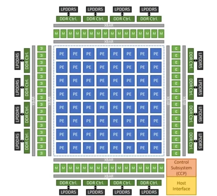
(referenced from the paper: MTIA: First Generation Silicon Targeting Meta’s Recommendation Systems)
The Growing NoC Latency Challenge
As AI chips grow larger and more complex, accelerator blocks are spread further across the die, connected by Networks-on-Chip (NoC). An MMIO access to a block on the far side of the NoC can take 50 ─ 200+ cycles just for routing, and even longer under congestion. This makes the CPU’s outstanding MMIO transaction capability a meaningful factor in overall system throughput.
3. FlatBuffers: A Memory Subsystem Stress Test
We chose Google’s FlatBuffers library not as a representative AI workload, but as a stress test for the CPU memory subsystem. FlatBuffers is an open-source, cross-platform serialization library designed for zero-copy data access, meaning it reads serialized data in place, without a separate deserialization step. While this library design is efficient in many respects, it creates memory access patterns that are particularly challenging for CPU caches and memory subsystems.
What Makes FlatBuffers Demanding
FlatBuffers uses indirect, offset-based data navigation: accessing any field requires reading an offset, computing a field address, and then following that address to the actual data. This results in multiple dependent memory accesses per field lookup. The read path, in particular, involves classic pointer chasing, which means each access depends on the result of the previous one. The chasing depth is configurable and can be set to a high value (e.g., 2000), meaning the traversal spans far more data than a single cache line can hold. As a result, cache misses are frequent and unpredictable. Accesses tend to be small and scattered, touching a few bytes at one location before jumping to an entirely different cache line. Combined with extensive small function calls for field accessors, FlatBuffers stresses the instruction cache, branch predictor, and memory subsystem simultaneously.
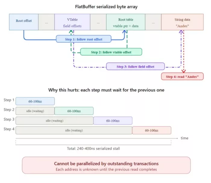
Figure 2. Flatbuffer read
Establishing a Performance Floor
By evaluating under these deliberately demanding conditions, we establish a performance floor for the CPU. Real-world workloads, which typically exhibit more regularity and spatial locality, can be expected to benefit even more from the core’s architectural features for latency tolerance.
4. What We Learned: Outstanding Transactions Under Two Access Patterns
Our evaluation on the Andes AX46MPV RISC-V core revealed that the architectural benefit of outstanding transactions varies dramatically depending on the memory access pattern, not just the cache miss rate.
FlatBuffer Create: Independent Accesses, High Benefit
In the FlatBuffer Create kernel, the CPU allocates buffers, writes fields, and builds the serialized data structure. These memory accesses are largely independent of each other, that is, the address of one write does not depend on the result of a previous read. Despite a low DRAM access frequency of just 0.23% (shared cache misses as a proportion of total instructions), the core achieved a 20% to 39% performance benefit from its outstanding transaction capability. The range depends on how we model the worst case without outstanding transactions. The upper bound of 39% assumes every DRAM access fully stalls the pipeline for the entire memory latency with no instruction overlap whatsoever, which is a deliberately pessimistic assumption. The lower bound of 20% assumes that some instructions can still be executed during a DRAM stall, effectively halving the DRAM access cycles. The actual benefit likely falls somewhere within this range, but even at the conservative end, a 20% gain from just a 0.23% miss rate demonstrates that when cache misses are independent, the hardware can issue multiple requests simultaneously and continue useful work while waiting. This is the ideal scenario for memory-level parallelism: rare but independent misses that can be fully overlapped.
FlatBuffer Read: Pointer Chasing, Limited Benefit
The FlatBuffer Read kernel tells a very different story. This workload is dominated by pointer chasing. The CPU reads an offset, dereferences it to compute the next address, reads that location, follows the next offset, and so on. Each memory access depends on the result of the previous one, creating a strict chain of data dependencies. Despite a much higher DRAM access frequency of 1.99%, the core achieved only a 6% performance benefit from outstanding transactions. The small gain likely comes from brief windows where the access pattern allows limited parallelism. Perhaps when reading multiple independent fields within a single FlatBuffer object after resolving its base pointer. But the dominant pointer-chasing pattern fundamentally limits how much latency the hardware is able to hide.
The Key Insight: Not All Cache Misses Are Equal
This contrast carries an important implication for system architects and workload designers. The value of outstanding transaction capability depends not on how many cache misses occur, but on whether those misses are sufficiently independent to be overlapped. Workloads with parallel, unrelated memory accesses can see dramatic benefits; workloads with serialized, data-dependent accesses will see far less improvement, regardless of how many outstanding transactions the hardware supports.
5. Beyond Outstanding Transactions: Prefetching as a Complementary Strategy
Outstanding transactions are most effective when cache misses are independent and can be issued in parallel. However, not all workloads exhibit this pattern. When the access pattern has some regularity but not enough parallelism to exploit, outstanding transactions alone are insufficient. This is where prefetching can provide partial relief.
The Andes AX46MPV includes both hardware prefetch and software prefetch capabilities. Hardware prefetching detects regular access patterns, such as sequential or strided accesses, and speculatively fetches data into the cache before the core requests it. Software prefetch instructions give programmers explicit control, allowing them to insert prefetch hints at strategic points in the code where the hardware prefetcher cannot anticipate the access pattern on its own.
Together with outstanding transactions, these prefetch mechanisms form a multi-layered defense against memory latency, each addressing a different dimension of the problem.
6. Conclusion: A Multi-Dimensional Approach to the Memory Wall
When cache misses occur in a modern SoC, whether to cacheable DRAM or to uncacheable MMIO device registers across a complex interconnect, the resulting latency is a multi-dimensional problem. No single feature eliminates it. The Andes AX46MPV architecture addresses this challenge from multiple angles: outstanding transactions exploit memory-level parallelism when access patterns allow it, hardware prefetching predicts and fetches data before the core needs it, and software prefetch gives developers an additional tool to partially overlap latency.
Our FlatBuffers evaluation makes this concrete: outstanding transactions deliver a 20 ─ 39% gain when cache misses are independent, but under pointer-chasing patterns, the benefit drops to 6%. For SoC designers, this underscores a practical truth: understanding your workload’s access patterns is just as important as the hardware features themselves. For those building the next generation of AI, automotive, and data center platforms, this kind of comprehensive, multi-dimensional latency tolerance is not a luxury. It is a necessity.
7. Acknowledgement
This article would not have been possible without the support of several colleagues. The CCBU team carried out the FPGA measurements that underpin our evaluation. Our NA team provided thoughtful reviews and suggestions that helped sharpen this article. Our knowledgeable architect and R&D team behind the AX46MPV were always willing to discuss the questions and challenges we encountered during benchmark analysis with us. Thank you all.
Author:
Mia Chang is a solution architect at Andes Technology with more than 10 years of experience spanning semiconductor circuit modeling and CPU synthesis. She works directly with AI compute and automotive customers, performing in-depth kernel-level analysis to uncover performance bottlenecks in real-world system designs.
About Andes Technology
As a Founding Premier member of RISC-V International and a leader in commercial CPU IP, Andes Technology is driving the global adoption of RISC-V. Andes’ extensive RISC-V Processor IP portfolio spans from ultra-efficient 32-bit CPUs to high-performance 64-bit Out-of-Order multiprocessor coherent clusters. With advanced vector processing, DSP capabilities, the powerful Andes Automated Custom Extension (ACE) framework, end-to-end AI hardware/software stack, ISO 26262 certification with full compliance, and a robust software ecosystem, Andes unlocks the full potential of RISC-V, empowering customers to accelerate innovation across AI, automotive, communications, consumer electronics, data centers, and mobile devices. Over 20 billion Andes-powered SoCs are driving innovations globally. Discover more at www.andestech.com.
Related Semiconductor IP
- 64 bit RISC-V Multicore Processor with 2048-bit VLEN and AMM
- 32-bit 8-stage superscalar processor that supports RISC-V specification, including GCNP and Linux
- 64-Bit 8-stage superscalar RISC-V processor
- Compact High-Speed 32-bit CPU for Real-time and Linux Applications
- Compact High-Speed 64-bit CPU for Real-time and Linux Applications
Related Blogs
- High Capacity and High Performance Flash Memory
- New Arm Cortex-A77 CPU continues path towards compute performance leadership
- Adding RISC-V CPU Custom Extensions Can Boost Performance, Reduce Power, and Cut Cost in 5G, AI. AR/VR, and IoT applications
- Cortex-X: The X-factor in Arm's CPU performance trajectory