Vendor: Floadia Corporation Category: MTP

Zero Additional Mask MTP

LEE Flash ZT (ZT) achieves automotive grade temperature and quality grade.

HHGrace 180nm BCD In Production View all specifications

Overview

LEE Flash ZT (ZT) achieves automotive grade temperature and quality grade.

Perfect fit for trimming and parameter storage in Sensor, Power and Analog ICs especially for automotive applications.

It also achieves low cost implementation due to its very short test time and baking time while you need Zero additional mask or process step in manufacturing.

It supports process nodes down to around 40nm and P/E cycle up to 10K times.

Item Spec
Process platform 180BCD
Memory Size 512 Bytes(4K bits)
P/E Cycles > 100k
Supply Voltage VDD 2.5V~5.5V
Additional Masks 0
Operation Temperature(Tj) -40~150℃
Data Retention

20years@-40~150℃


High Temperature Operation

ZT can support 20 years of retention at 125°C. ZT has track record in supporting Automotive quality.

Large Program Size enables Short Testing Time

ZT uses FN tunneling technology to achieve extremely low power in program and erase.
It consumes 1/1,000,000 times current, compared to conventional technologies which use hot carrier injection for program/erase operation.
This also helps reducing testing time, which dominates large portion of the chip cost.

Low Cost

Short Test Time: ZT achieves very short test time for two reasons.

  • Extremely low power in program/erase allows tester to program/erase the whole memory mat at once, compared to conventional solution program/erase smaller sections for many many times to program/erase the whole memory mat.
  • Sharp Vt distribution in programming will eliminate the requirement for multiple programming and verification, so that programming operation always completes at one time, not in multiple steps, to dramatically reduce programming time.

Short Baking Time

Floadia’s unique memory architecture simplifies Life Time Prediction of the memory cell, which allows chip company to screen devices with shorter baking time.

Zero Mask

ZT requires no change and no additional mask on standard CMOS process, reducing expensive mask cost to implement NVM feature on your chip.

Field Programmability

Floadia’s ZT allows system company to program NVM when they ship end system product, or even while the system is in the field and running, to adjust trimming/parameter setting.
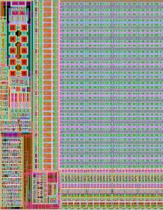

Key features

  • Supports high temperature and long retention life time for severe automotive requirement.
  • Low power in Program/Erase operation for power critical applications.
  • Short Test and Bake time to reduce chip cost.
  • Standard CMOS process for re-using existing design and IP.
  • No additional mask required for easy implementation.

Block Diagram

Silicon Options

Foundry Node Process Maturity
HHGrace 180nm BCD In Production

Specifications

Identity

Part Number
LEE Flash-ZT
Vendor
Floadia Corporation
Type
Silicon IP

Files

Note: some files may require an NDA depending on provider policy.

Provider

Floadia Corporation
HQ: Japan
Established in 2011, Floadia is a spin-out of experienced engineers who were developing embedded memory at Renesas Electronics Corporation for more than 20 years. The company licenses its intellectual property (IP), including manufacturing process and circuit designs, necessary for the embedded memory production. Floadia’s development team comprises not only circuit designers but also engineers with expertise in the manufacturing process. One of the company’s strengths is its ability to develop optimal memory IP according to customer’s specifications and manufacturing process. As battery-powered devices such as smart phones and tablet rapidly become more feature-rich and sophisticated, the memory, one of a key component is required to reduce its cost, power consumption and geometry. The demand for Non-Volatile Memory* (eNVM) is increasing due to its wide range of applications including program and data storage, performance tuning (trimming), and storage of encryption keys. Floadia has developed the technology to embed NVM within other operational circuit while minimizing additional manufacturing process and hence enables IC and microcontroller manufacturer to reduce cost and geometry dramatically. Furthermore, as Floadia’s eNVM uses FN tunneling** for data writing, power consumption per memory cell can be reduced by 100,000 to 1,000,000 times. The Internet of Things (IoT) is expected to become more pervasive and as a key component of IoT products, memory is indispensable. Floadia’s low-cost, low-power-consumption memory can facilitate the mass deployment of IoT devices such as beacons and various sensors. It can also enhance the profitability of IoT business and contribute to the major expansion of the IoT market. Manufacturing costs have risen for semiconductor foundries and fabless companies as the miniaturization of silicon process design rule advances further. The installation of Floadia’s versatile and user-friendly memory allows these companies to reduce not only costs, but also the time to reach mass production.

Learn more about MTP IP core

How to Elevate RRAM and MRAM Design Experience to the Next Level

This article will explore the potential advantages of RRAM and MRAM in various applications and elucidate why such new technologies are imperative to address future memory demands, as well as some challenges designers may encounter in the implementation.

Unleashing EEPROM Potential by Going Embedded: Introducing eMemory's NeoEE

EEPROM memory, which recently celebrated its 50th birthday, continues to defy obsolescence. Despite its age, EEPROM remains a mature, reliable, and affordable technology for many electronic systems. As IC designers embed EEPROM onto chips, it has become an integral part of chip design, offering essential benefits to applications such as MCU, PMIC, sensors, and RFID tags.

Calibrate and Configure your Power Management IC with NVM IP

Power Management Integrated Circuits (PMICs) are the first to turn on and the last to turn off in a system. They perform the task of delivering the right voltage to component chips by regulating or boosting the voltage levels to the component chips.

How eNVM Helps Power Controllers Be Smarter

PMIC designers have learned that using eNVMs like OTP in their chips can be very beneficial. A simple state machine with OTP can store power sequences and parameters, which can help manage the power between ICs efficiently.

NVM memory: A Critical Design Consideration for IoT Applications

The explosion of information that IoT devices will gather will require huge numbers of processors to process and manage the data from these IoT devices along with lots of low-cost, secure and reliable embedded non-volatile memory (NVM) for code storage, sensor trimming, device configuration, security keys and other storage functions. Virtually every one of the projected billions of IoT devices can use some amount of one-time programmable (OTP) memory.

Frequently asked questions about MTP Memory IP cores

What is Zero Additional Mask MTP?

Zero Additional Mask MTP is a MTP IP core from Floadia Corporation listed on Semi IP Hub. It is listed with support for hhgrace In Production.

How should engineers evaluate this MTP?

Engineers should review the overview, key features, supported foundries and nodes, maturity, deliverables, and provider information before shortlisting this MTP IP.

Can this semiconductor IP be compared with similar products?

Yes. Buyers can compare this product with similar semiconductor IP cores or IP families based on category, provider, process options, and structured technical specifications.

×
Semiconductor IP