Vendor: Cadence Design Systems, Inc. Category: SRAM

Simulation VIP for OSPI NOR

In production since 2012 for dozens of designs.The Cadence® Memory Model Verification IP (VIP) for Flash Octal SPI (OSPI) Flash p…

Verification IP View all specifications

Overview

In production since 2012 for dozens of designs.

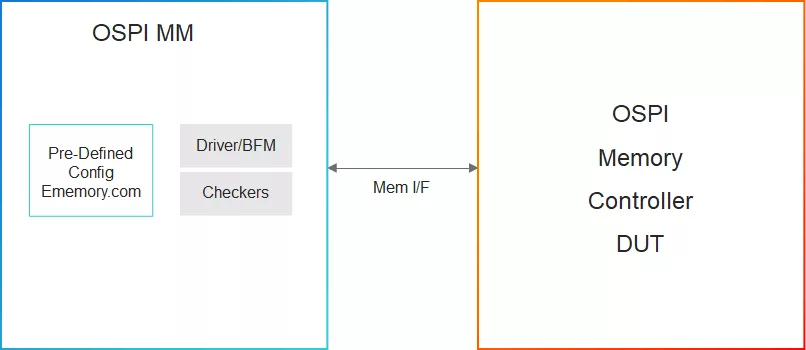
The Cadence® Memory Model Verification IP (VIP) for Flash Octal SPI (OSPI) Flash provides verification of serial flash NOR devices using the SPI protocol. The OSPI VIP is compatible with the industry-standard Universal Verification Methodology (UVM), runs on all leading simulators, and leverages the industry-standard Cadence Memory Model core architecture, interface, and use model.

Supported Specification: Octal SPI features of the vendors: Micron, Macronix, Adesto, ISSI, and GigaDevices.
Key features

  • Device Density
    • From 256Mb to 2Gb, with frequency up to 133MHz in SPI and 200MHz in OSPI mode
  • Operation Mode
    • Extended SPI mode, Octal SDR and DDR mode (Single I/O and Octal I/O)
  • RESET
    • Software Reset: RESET and RESETN command, as well as Hardware Reset using the Reset Pin
  • Read ID
    • Read Serial Flash Discoverable parameter
  • XIP
    • Execute-in-place (XIP), Fast Boot feature after Power on cycle or Reset
  • Configuration
    • Configuration registers Read and Write for Volatile and Non-volatile registers
    • Configuration Capability: Volatile and non-volatile configuration register settings to change the mode of the model, Dummy cycles for read commands, 3-byte or 4-byte addressing, Output Drive Strength (ODS), DQS Enable and Disable, ECC enable and disable, CRC enable and disable, Wrap enable and disable, and Wrap size
  • Addressing Capability
    • 3-byte and 4-byte address modes enable memory access beyond 128Mb
  • Commands
    • Supports Read (SPI), Fast Read, Octal Output Read, Octal I/O Fast Read, DDR Octal Output Fast read, and DDR Octal I/O Fast Read (DDR mode only)
    • Supports Burst Read by using Set Burst Length command you can set 16-byte, 32-byte, or 64-byte Wrap Bursts for Read commands
    • Supports Page Program, Sub-Sector Erase with 4KB and 32KB granularity, Sector Erase with uniform granularity and Bulk (Chip) Erase commands
    • Supports Buffer Write (84h), Buffer Read (D4h), Buffer to Main Memory Page Program without Built-In Erase, WP pin functionalities (signals are shared with I/O pins), Echo (AAh), Echo with Inversion (A5h) (Adesto Specific)
    • Support Program, Erase Suspend and Resume operations, Support Deep Power Down mode
    • DDR Center Aligned Read Strobe (DCARS) : DQs is driven on 90-degree phase-shifted clock (sclk2) rather than actual clock (sclk)
    • Interruptible Write Buffer: Write Buffer Initial (WRBI), Write Buffer Continue (WRCT), Write Buffer Confirm (WRCF) and Page Buffer Read (RDBUF)
    • Timing: Supports Device Input and Output timing and Variants memory operations timing (for Program, Erase, Suspend, and Resume)
  • Preamble Pattern
    • Based on the PBE bit value, selected Preamble Pattern will be inputted to the Dummy Cycles
  • Security and Write Protection
    • Volatile and nonvolatile locking and software Write Protection for each 128KB sector:
    • Hardware write protection: Based non-volatile bits defined protected area size, Program and erase protection during power-up, CRC detects accidental changes to raw data
  • Read While Write
    • Divides into 2 banks or 4 banks of 0-32Mbit each: While an Erase or Program operation is taking place in one bank, a Read can take place in other
  • OTP
    • Readable, user-lockable 64bytes to 8K-bit Security OTP memory outside main memory and Permanent lock with PROGRAM OTP command

Block Diagram

Specifications

Identity

Part Number
Simulation VIP for OSPI NOR
Vendor
Cadence Design Systems, Inc.
Type
Verification IP

Files

Note: some files may require an NDA depending on provider policy.

Provider

Learn more about SRAM IP core

DDR5 MRDIMM Gen2: The Missing Link in Scaling AI Infrastructure

Cadence leads the market with its DDR5 MRDIMM 12.8 Gbps Gen2, TSMC N3P IP system solution, establishing a new benchmark for industry-leading PPA. Key industry leaders have already adopted this solution, which is now also available in the TSMC N2P and N5/N4P process nodes.

AI Semiconductor Design at 3nm and 2nm: Silicon-Proven IP

In this second blog of our ongoing series, we examine how Cadence, in close partnership with TSMC, helps teams accelerate AI silicon design at advanced process nodes. For customers, this translates into reduced design risk, faster convergence to tapeout‑quality results, and greater confidence at the leading edge of AI and HPC design.

Frequently asked questions about SRAM IP cores

What is Simulation VIP for OSPI NOR?

Simulation VIP for OSPI NOR is a SRAM IP core from Cadence Design Systems, Inc. listed on Semi IP Hub.

How should engineers evaluate this SRAM?

Engineers should review the overview, key features, supported foundries and nodes, maturity, deliverables, and provider information before shortlisting this SRAM IP.

Can this semiconductor IP be compared with similar products?

Yes. Buyers can compare this product with similar semiconductor IP cores or IP families based on category, provider, process options, and structured technical specifications.

×
Semiconductor IP