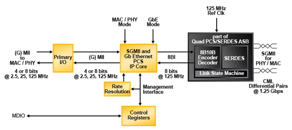
Overview
The Lattice SGMII and Gb Ethernet PCS IP core implements the PCS functions of both the Cisco SGMII and the IEEE 802.3z (1000BaseX) specifications. The PCS mode is pin selectable. This IP core may be used in bridging applications and/or PHY implementations.
The Serial Gigabit Media Independent Interface (SGMII) is a connection bus for Ethernet Media Access Controllers (MACs) and Physical Layer Devices (PHYs) defined by Cisco Systems. It replaces the classic 22-wire GMII connection with a low pin count, 4-pair, differential SGMII connection. The classic GMII interface defined in the IEEE802.3 specification is strictly for Gigabit rate operation. However, the Cisco SGMII specification defines a method for operating 10 Mbps and 100 Mbps MACs over the interface. Moreover, the Cisco SGMII specification is comprised of more than just a bus interface definition; it defines a bridging function between SGMII and GMII buses.
These applications can be completely implemented in ECP5, LatticeECP3™, LatticeECP2M™ and LatticeSC™ Field Programmable Gate Array (FPGA) devices. As an example, Lattice has developed a reference design for a complete SGMII-to-(G)MII bridge. This reference design is included with the SGMII and Gb Ethernet PCS IP Core package and is described in detail in Appendix C.
The core can be instantiated, synthesized and simulated through IPexpress™ software.
Learn more about Single-Protocol PHY IP core
Extending Lattice's post-quantum cryptography leadership from silicon to a complete platform security stack, Lattice Sentry now delivers CNSA 2.0-aligned, NIST-compliant protection across AI data centers, and critical infrastructure, giving system designers a validated, production-ready path to quantum-resistant security.
Combining Arm® AGI CPU server platforms with Lattice FPGAs and AMI firmware creates a solution that provides advanced security, manageability, connectivity, and flexibility for next-generation AI data center infrastructure.
Lattice Prompt pairs with AI agentic tools developers already use, combining them with Lattice design tools, knowledge base, and documentation to turn natural language inputs into validated responses, dramatically accelerating FPGA development while optimizing design performance and capability.
First announced on May 4, 2026, the acquisition creates the industry's most complete secure management and control platform.
The acquisition brings together Lattice’s industry-leading low power FPGAs with AMI’s industry‑leading platform firmware and infrastructure manageability solutions for cloud and AI to create a complete portfolio of secure management and control solutions.
The collaboration demonstrates a real-time AI sensor fusion architecture that integrates TI mmWave radar and camera sensors using NVIDIA Holoscan Sensor Bridge running on Lattice’s low power FPGA. The FPGA acts as a companion chip delivering synchronized sensor data directly into GPU-accessible memory to enable low-latency and robust perception for robotics and industrial edge AI applications.