Vendor: T2M GmbH Category: Multi-Protocol PHY

PCIe 2.0 Serdes PHY IP, Silicon Proven in SMIC 40LL

PCIe Gen 2 PHY IP is a physical layer (PHY) IP solution for consumer electronics, that allows for a full featured customization a…

SMIC 40nm LL In Production View all specifications

Overview

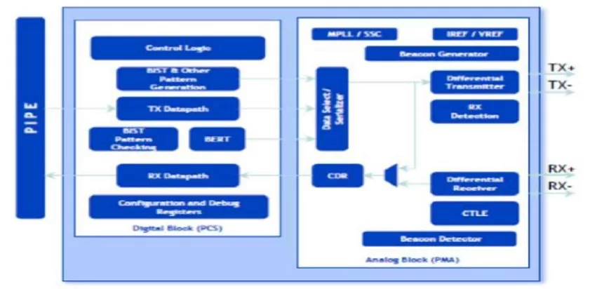
PCIe Gen 2 PHY IP is a physical layer (PHY) IP solution for consumer electronics, that allows for a full featured customization and complies with the PCIe2.0 fundamental specifications while incorporating mixed signal circuits to provide 2.5GT/s and 5.0GT/s data transfer speeds. Physical Media Attachment (PMA) and Physical Coding Sublayer (PCS) are the two levels that make up the PCIe2.0 PHY IP. It simply connects to either the PCIe2.0 MAC layer utilizing the industry-standard PIPE-3.0 interface.
The PCIe2.0 PHY IP transceiver is optimized for low power consumption and small die area while retaining great result and data throughput. The PCIe2.0 PHY IP includes an on-chip physical transceiver solution with ESD protection, a built-in self-test module with inbuilt jitter injection, and a dynamic normalization circuit that ensures full support for high-performance configurations.

Key features

  • Compatible with PCIe base Specification
  • Full compatible with PIPE4.2 interface specification
  • Independent channel power down control
  • Implemented Receiver equalization Adaptive-CTLE to compensate insertion loss
  • Support 16-bit/32bit parallel interface
  • Support for PCIe gen1(2.5Gbps) and PCIe gen2(5.0Gbps)
  • Support flexible reference clock frequency
  • Support 100MHz differential reference clock input or output (with SSC optionally) in PCIe Mode
  • Support Spread-Spectrum clock (SSC) generation and receiving from -5000ppm to 0ppm
  • Support programmable transmit amplitude and Deemphasis
  • Support TX detect RX function in PCIe Mode
  • Support Beacon signal generation and detection in
  • Production test support is optimized through high coverage at-speed BIST and loopback
  • Integrated on-die termination resistors and IO Pads/Bumps
  • Embedded Primary & Secondary ESD Protection
  • ESD: HBM/MM/CDM/Latch Up 2000V/200V/500V/100mA
  • Silicon Proven in SMIC 40LL

Block Diagram

What’s Included?

  • GDSII & layer map
  • Place-Route views (.LEF)
  • Liberty library (.lib)
  • Verilog behaviour model
  • Netlist & SDF timing
  • Layout guidelines, application notes
  • LVS/DRC verification reports

Silicon Options

Foundry Node Process Maturity
SMIC 40nm LL In Production

Specifications

Identity

Part Number
PCIe 2.0 Serdes PHY IP in 40LL
Vendor
T2M GmbH
Type
Silicon IP

Files

Note: some files may require an NDA depending on provider policy.

Provider

HQ: Germany

Learn more about Multi-Protocol PHY IP core

Three Design Aspects you shouldn't miss while building an NB-IoT Protocol Stack

It is very important that the design aspects of the NB-IoT device protocol stack ensure low module cost and low energy consumption. This is required to match the industry expected module costs. This paper outlines some of the NB-IoT Protocol stack specification flexibilities and generic design aspects that are to be considered to meet the above requirements, especially with reference to LTE.

Frequently asked questions about Multi-Protocol PHY IP cores

What is PCIe 2.0 Serdes PHY IP, Silicon Proven in SMIC 40LL?

PCIe 2.0 Serdes PHY IP, Silicon Proven in SMIC 40LL is a Multi-Protocol PHY IP core from T2M GmbH listed on Semi IP Hub. It is listed with support for smic In Production.

How should engineers evaluate this Multi-Protocol PHY?

Engineers should review the overview, key features, supported foundries and nodes, maturity, deliverables, and provider information before shortlisting this Multi-Protocol PHY IP.

Can this semiconductor IP be compared with similar products?

Yes. Buyers can compare this product with similar semiconductor IP cores or IP families based on category, provider, process options, and structured technical specifications.

×
Semiconductor IP